


News: Microelectronics
27 August 2020
Halogen-free vapor phase epitaxy for GaN
Toyota Central R&D Labs Inc in Japan has been developing a halogen-free vapor phase epitaxy process for gallium nitride (GaN) with a view to power devices with high breakdown voltage (1200V and above) [Taishi Kimura et al, Appl. Phys. Express, vol13, p085509, 2020].
“Our study shows that the HF-VPE technique can be employed to achieve high-quality and cost-effective bulk crystal and epitaxial layer growth for GaN devices,” reports the team, which included researchers from University of Tsukuba and Nagoya University in Japan, in addition to the Toyota personnel.
In many respects, the material had performance comparable to that obtained from low-defect-density hydride vapor phase epitaxy (HVPE).
The HVPE process involves reacting group III metals (e.g. Ga) with hydrogen chloride (HCl), producing gaseous chlorides (GaCl, for instance). The epitaxy then proceeds through reaction with ammonia (NH3).
The halogen-free vapor phase epitaxy (HF-VPE) process instead uses direct reaction of the group-III metal in gaseous form with NH3:
Ga(g) + NH3 → GaN(s) + 3/2H2
This avoids the production of ammonium chloride (NH4Cl), which clogs up production equipment, and needs frequent chamber cleaning processes, which interrupts manufacturing, increasing costs.
The researchers built on their previous work, producing HF-VPE GaN layers on commercial freestanding GaN and GaN/sapphire templates. The templates were from a metal-organic chemical vapor deposition (MOCVD) process.
The team avoided dislocation formation at the initial growth interface by carefully controlling the process conditions: substrate holder at 1283-1393K, source crucible at 1530-1537K, and 2kPa growth pressure. The crucible was heated using radio-frequency irradiation.
The aim was to eliminate void-like defects, which have been found to be a prime source of interface dislocations. The carrier, sheath, diluent and reaction gases were supplied at 0.3 standard liter per minute (slm) N2, 0.2slm N2, 1.6-5.0 slm N2, and 1.0-4.0slm NH3. The researchers targeted a relatively low 30-40μm/hour growth rate.
X-ray study revealed little difference in the width of rocking curves between the substrates and the overlying HF-VPE GaN layers, suggesting minimal addition of dislocations at the initial growth interface. The team also points out that they found no evidence of Ga inclusions in the HF-VPE material – Ga inclusions are another source of crystal defects in GaN.
Secondary-ion mass spectroscopy showed hydrogen, oxygen and carbon at a sub-background impurity level in the HF-VPE layer: less than 3x10¹⁶/cm3, 8x10¹⁵/cm3 and 6x10¹⁵/cm3, respectively.
The silicon (Si) impurity level did increase somewhat – to around 2x10¹⁷/cm3. In vertical-conduction power devices, it is often desired to have thick drift layers with the Si concentration as low as possible. The researchers comment: “These unintentional Si impurities (typically 1016-1017/cm3) could be attributed to the quartz parts located in the high-temperature region in the HF-VPE apparatus. A modified growth setup is currently being developed to reduce Si.”
Hall measurements were carried out on HF-VPE layers grown on high-resistivity MOCVD GaN/sapphire templates. The HVPE freestanding substrates were conductive, and therefore not suitable for accurate Hall analysis of carrier concentration and mobility.
The varying free-electron concentration was achieved using Si doping, which was well controlled above 1017/cm3 level up to 1019/cm3 (Figure 1). Lower free-electron levels would need the modified growth setup referred to above.
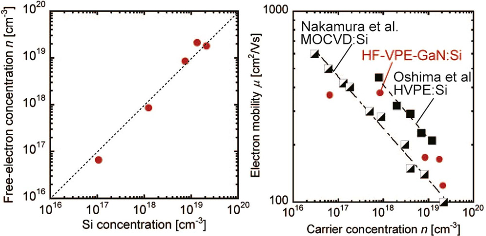
Figure 1: Relationship between Si and net donor (Nd-Na) concentrations for Si-doped HF-VPE GaN (left). Dependence of electron mobility on carrier concentration for GaN layers at 300K (right).
The mobility measurements were compared with MOCVD- and HVPE-grown n-GaN layers by other groups. The HF-VPE generally showed improved mobility performance over MOCVD GaN, except at the lowest free-carrier concentration (6.6x10¹⁶/cm3). However, the HVPE GaN comparison was better.
The team explained the reduced mobility performance, compared with the HVPE report, as probably arising from the high dislocation density of the MOCVD template used. MOCVD GaN dislocation densities are of the order 1-3x10⁹/cm2, while HVPE achieves much reduced dislocation generation around 3-5x10⁶/cm2.
The low mobility of the HF-VPE GaN at the lowest electron concentration could be due to the presence of acceptor-like compensating impurities or Ga vacancy point defects, degrading the performance.
Positron annihilation spectroscopy (PAS) confirmed there was a particular problem for HF-VPE layers grown on MOCVD GaN/sapphire templates.
The ‘S-parameter’ was higher on the templates than for material grown on freestanding GaN – 0.445, compared with 0.442, using 28.6keV incident positrons. The S-parameter compares the gamma-ray photon emissions (~511keV) from electron-positron emissions from the central peak region with the total emissions. Annihilation with less mobile electrons reduces Doppler broadening. A high S-parameter therefore indicates the presence of more electrons trapped at electroneutral or negatively charged vacancy-type defects.
Analyzing the S-parameter versus incident positron energy behavior allowed extraction of positron diffusion lengths. This was highest for HVPE material ~100nm. The HF-VPE process on freestanding GaN reduced the diffusion length to the range 70-80nm. The material on MOCVD templates gave a value of ~40nm.
Positron diffusion lengths are reduced both by positron trapping by vacancy-type defects and positron scattering by impurities.
Using a two-state trapping model, the researchers estimated a Ga vacancy complex density (VGa) on MOCVD templates of ~1017/cm3.
The deep-level defects were explored by cathodoluminescence (CL) – studying light emission from irradiation with a 5keV electron beam (Figure 2). The spectra showed near-ultraviolet peaks associated with free exciton (FX, 3.48eV), donor-bound exciton (DBE, 3.47eV), and longitudinal optical (LO) phonon replicas of FX (3.39, 3.30, and 3.21eV) near-band-edge emissions.
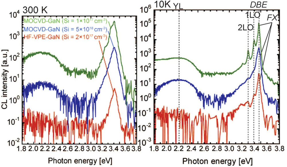
Figure 2: CL spectra for HF-VPE-GaN at 300K (left) and 10K (right). Spectra for Si-doped MOCVD-grown GaN also shown. The spectra for Si-doped MOCVD-grown GaN are shifted upward by factors of 10 and 100 for clarity.
In MOCVD GaN one also finds a broad ‘yellow luminescence’ (YL) hump (2.2-2.3eV), which is associated with deep-level defects. The level of YL in HF-HVPE was at least an order of magnitude lower than for MOCVD GaN.
The researchers comment: “Although the origin of YL peaks is still under discussion, many researchers have reported that it originates from complexes in which gallium vacancies are related to oxygen (VGa-ON) and/or carbon (VGa-CN).”
Oxygen and carbon are unavoidable in metal-organic CVD processes. Quartz equipment can also contribute oxygen. The researchers comment: “The absence of a YL peak is attributable to the high-purity (O-free and C-free) growth of the HF-VPE method.”
The researchers see the slightly lower PAS diffusion length and CL intensity of HF-VPE GaN compared with HVPE GaN as indicative that other impurities may be present in HF-VPE GaN layers, whose identification and removal could raise electron mobility and CL intensity in HF-VPE-GaN.
https://doi.org/10.35848/1882-0786/aba494
The author Mike Cooke is a freelance technology journalist who has worked in the semiconductor and advanced technology sectors since 1997.


