


News: Optoelectronics
6 August 2020
CW operation of semi-polar GaN-on-sapphire laser
University of California Santa Barbara (UCSB) in the USA claims the first continuous-wave (CW) electrically driven semi-polar gallium nitride (GaN) blue laser diodes (LDs) at room temperature heteroepitaxially grown on 4-inch sapphire substrate [Haojun Zhang et al, ACS Photonics, vol7, p1662, 2020]. The researchers see their work as “a significant breakthrough in substantially reducing the cost of semi-polar laser diodes and expediting the development of future semi-polar GaN laser diodes and their applications”.
The semi-polar GaN crystal orientation enables the growth of indium gallium nitride (InGaN) light-emitting layers with a more efficient recombination of electrons and holes into photons, compared with the conventional charge-polarized c-plane orientation. Also, the hole mobility in semi-polar materials is higher, improving injection into light-emitting structures. Emissions also tend to be optically polarized – a property that could also be useful for device applications.
The team sees potential benefits from semi-polar laser diodes for applications such as LiFi light communications, where very high data rates of 20Gbits/second have been demonstrated, beyond the performance of 5G wireless.
Up to now semi-polar light-emitting devices have been realized mainly through homoepitaxy on very expensive freestanding GaN substrates. Heteroepitaxy on sapphire would be much more cost-effective, but semi-polar material on such substrates has previously been of very low quality, making useful devices almost impossible to fabricate.
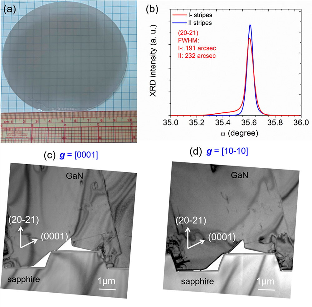
Figure 1: (a) Image of 4-inch (20-21) GaN on sapphire substrate; (b) x-ray diffraction rocking curves of on-axis (20-21) plane with axis perpendicular and parallel to patterned stripes; bright-field cross-sectional transmission electron microscope images under two-beam conditions along (c) g = [0001] and (d) g = [10-10] diffraction vectors with [11-20] zone axis.
The semi-polar (20-21) GaN layers were grown on (22-43) sapphire substrates using metal−organic chemical vapor deposition (MOCVD). The sapphire was patterned with 6μm trenches to expose the c-plane on the trench sidewalls before the GaN growth (Figure 1). The GaN/sapphire templates were supplied by Yale University spin-out company Saphlux Inc. On the basis of x-ray diffraction and transmission electron microscopy, the UCSB researchers estimate a threading dislocation density of ~1x10⁸/cm3.
The (20-21) template surface was planarized using chemical mechanical polishing (CMP). The laser diode structure (Figure 2) used a design without aluminium gallium nitride (AlGaN) cladding layers. AlGaN is slow to grow and has a large lattice mismatch with the rest of the III-nitride structure. There was a thin AlGaN electron-blocking layer (EBL) in the laser diode design.
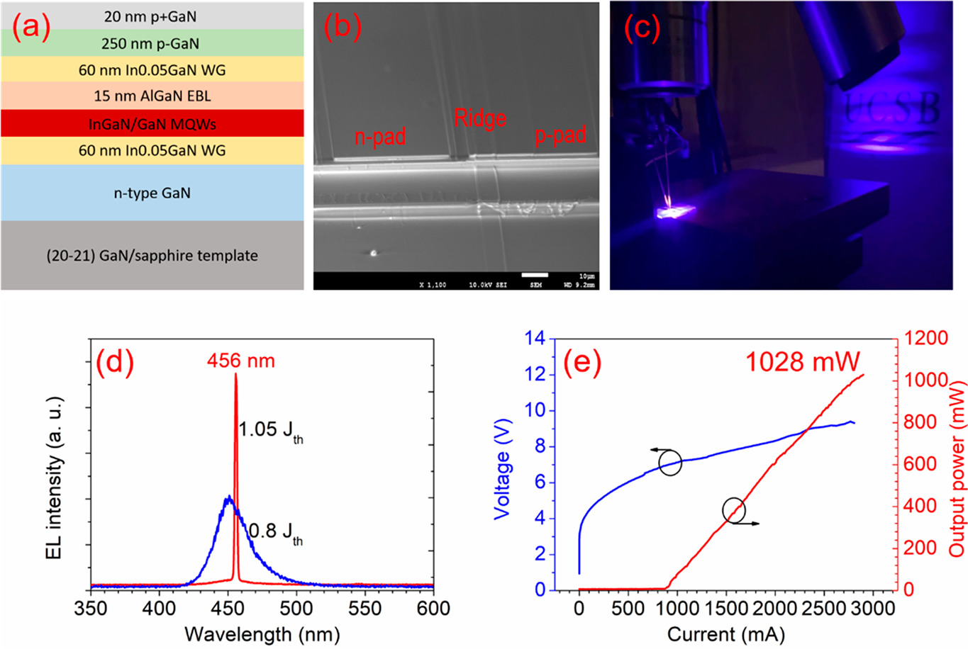
Figure 2: (a) Laser diode structure; (b) scanning electron micrograph of 1800μmx8μm laser diode; (c) electroluminescence (EL) and far-field image of laser diodes above lasing threshold; (d) EL spectra with injection current density of 0.8x and 1.05x threshold; (e) light output power and voltage versus current of 1800μmx8μm laser diode under pulsed operation at room temperature.
The epitaxial structure with InGaN multiple quantum well (MQW) active region was also grown by MOCVD. A thin p-GaN cladding component (250+20nm in this case) has been found previously by the UCSB group to enhance laser diode voltage performance and thermal management. The cladding was completed with indium tin (Sn) oxide (ITO), deposited at high temperature and low tin-doping concentration.
Ridge laser diodes were fabricated with silicon dioxide isolation. The 150nm ITO cladding was added by electron-beam evaporation at 650°C of a 90:10%wt In2O3/SnO2 target. The n-type contact was titanium/aluminium/nickel/gold. The p-contact pads were titanium/gold. The devices used chemically assisted ion-beam etched facets.
For testing, the sapphire substrate was thinned to 50μm thickness, from ~650μm. Sapphire is thermally insulating, and thinning the material enables better heat dissipation, reducing self-heating from CW operation. The thinning process was in two steps: first polishing down to 90μm, followed by inductively coupled plasma etching to 50μm.
The test set up found the individual laser bars mounted on a copper block with indium/lead solder. The block was put on an electrically and thermally controlled copper stage.
With 500ns pulse operation at 0.05% duty cycle, the threshold current density for a 1800μmx8μm device was 6kA/cm2 (880mA).The forward voltage was 6.9V, and the wall-plug efficiency (WPE) reached 4.1% at 1100mA (1.1A).
The maximum light output power (P0) achieved was 1028mW (1.028W) from a single facet with 2.8A current injection. The team claims this as the “best” performance reported so far for a semi-polar LD grown heteroepitaxially on a foreign substrate.
The researchers comment: “The P0 over 1W of the semi-polar laser diodes grown on a sapphire substrate marks a significant breakthrough in exploring the low-cost and high-performance semi-polar laser diodes.”
CW operation was, of course, more challenging (Figure 3). Even so, the achievement of CW lasing constitutes “the world’s first report about heteroepitaxially grown CW semi-polar blue laser diodes on foreign substrates,” according to the researchers. The threshold of a smaller 1500μmx8μm laser diodes was 720mA (6kA/cm2). The WPE peaked at 2.5%. The P0 value was 243mW at 1.4A injection. The device was operated for an hour under CW conditions without noticeable performance degradation.
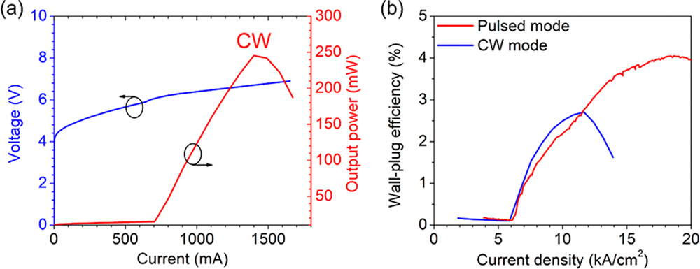
Figure 3: (a) Light output power and voltage versus current density for 1500μmx8μm laser diode under CW operation and (b) WPE performance for pulsed and CW modes.
The team believes that topside flip-chip bonding to a high thermally conductive substrate such as silicon carbide could significantly improve laser diode performance and WPE under CW operation.
Study of the optical polarization of the emissions showed it to be almost 100% transverse electric (TE), as opposed to transverse magnetic (TM), at 1100mA injection. This was expected behavior.
Semi-polar GaN blue laser diodes Blue laser diodes MOCVD GaN
https://dx.doi.org/10.1021/acsphotonics.0c00766
The author Mike Cooke is a freelance technology journalist who has worked in the semiconductor and advanced technology sectors since 1997.


