


News: Microelectronics
23 December 2020
Extreme-k and Ga2O3 power moves
Ohio State University in the USA has claimed the highest reported power figure of merit for gallium oxide (β-Ga2O3) lateral transistors of 376MW/cm2 [Nidhin Kurian Kalarickal et al, IEEE Transactions on Electron Devices, published online 1 December 2020]. The researchers used an insulator consisting of barium titanate (BaTiO3), a perovskite oxide that combines an extreme dielectric constant with high breakdown field strength (>8MV/cm).
The dielectric enabled a reduction in peak fields for a given bias, according to simulations. Radio frequency (RF) and power electronics could benefit from higher average electric fields enabling better efficiency, power density, and faster speed.
The team comments: “The integration of extreme permittivity dielectrics based on perovskite oxides into conventional and wide-bandgap semiconductors such as Si, GaAs, GaN and SiC could enable unprecedented performance improvements in RF and power electronics devices.”
The use of the BaTiO3 dielectric also enabled a higher channel charge density of 1.6x10¹³/cm2, reducing on-resistance. The β-Ga2O3 has a theoretical breakdown field strength of 8MV/cm, which is much greater than the 3MV/cm for gallium nitride (GaN). One drawback of β-Ga2O3 is a lower mobility. This can be compensated for somewhat with the higher channel charge.
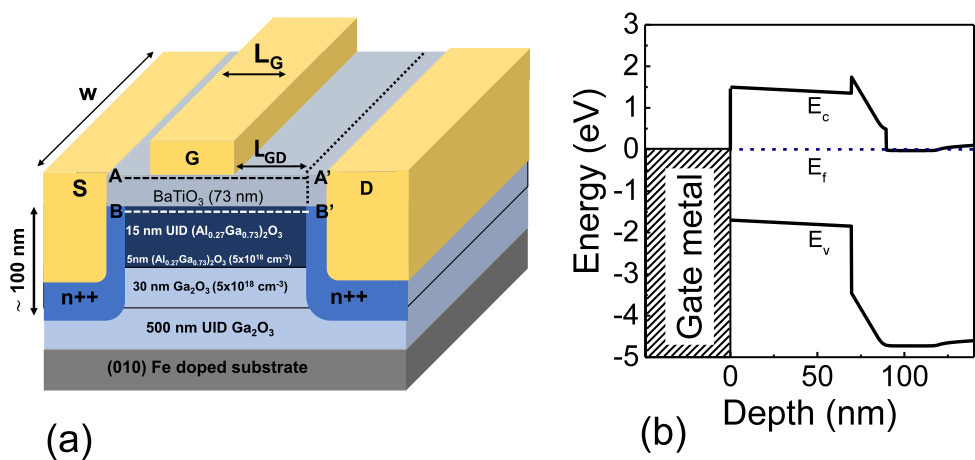
Figure 1: (a) Epitaxial/device diagram of BaTiO3/β-Ga2O3 MISFET. (b) Simulated band diagram along vertical cutline through gate.
The researchers fabricated lateral metal–insulator–semiconductor field-effect transistors (MISFETs) on β-Ga2O3 with extreme-k BaTiO3 as the insulator (Figure 1). The channel region was formed using 880°C metal-organic chemical vapor deposition (MOCVD) of β-(AlxGa1−x)2O3/Ga2O3 layers on iron-doped β-Ga2O3 substrate. The 5x10¹⁸/cm3 intentionally doped aluminium/gallium oxide layers were achieved with silicon from silane (SiH4).
Source and drain regions were defined using optical lithography followed by silicon ion implantation and activation by 900°C annealing for 30 minutes. The source and drain were then etched down to the β-Ga2O3 and annealed metal contacts formed from titanium/gold/nickel.
The BaTiO3 was applied using 670°C RF sputtering from a sintered BaTiO3 source. The BaTiO3 was 73nm thick, a little short of the 75nm target. The sputtering had a negative effect on the channel resistance, which the researchers hope could be ameliorated in the future with an Al2O3 interlayer to avoid sputter damage. The source/drain ohmic contacts also suffered from sputter degradation, which could be improved by applying the metals after the BaTiO3 and/or by optimizing the metal stack.
The device was completed with mesa isolation etching and deposition of a nickel/gold/nickel Schottky gate. The gate–drain spacings (Lgd) ranged from 0.5μm to 6μm. The gate length was 0.7μm.
Capacitance–voltage measurements suggested a dielectric constant of 235 for the BaTiO3, but the team comments: “This is only a lower bound estimate on the dielectric constant since there is a small depletion of charge in the channel after the deposition of BaTiO3. Nevertheless, the lower bound estimate of 235 is high enough to ensure electric field management.”
The lowest on-resistance was 13.6Ω-mm, normalized to the gate width with 0.5μm Lgd and 1.5μm Lsd. The drain current reached 359mA/mm – “the highest reported in any epitaxially grown β-Ga2O3 lateral transistor device under dc conditions, and higher currents have only been obtained in β-Ga2O3 nanomembrane transistors transferred onto high-thermal-conductivity substrates like diamond and Si,” according to the team.
The three-terminal breakdown voltage (Vbr) increases with Lgd, with the highest value being 918V for 6μm spacing. For 0.5μm Lgd breakdown occurred at 201V. The average field at breakdown reduced from 4MV/cm at 0.5μm Lgd to 1.5MV/cm at 6μm.
Reverse-bias current measurements suggested that gate leakage limited the breakdown performance. Simulations showed a spike in electric field at the gate corner, which in the device would increase gate current leakage and result in dielectric breakdown.
The power figure of merit Vbr2/RspON balances the trade-off of breakdown and specific on resistance, normalized to the source–drain area (Lsdxwidth). The devices all achieved a value for this figure of merit greater than 147MW/cm2, reaching 376MW/cm2 for 4.7μm Lsd and 3μm Lgd, which had 640V Vbr and 1.08mΩ-cm2 RspON. The team claims the 376MW/cm2 figure as “the highest reported value for any β-Ga2O3 transistor to the best of our knowledge” (Figure 2).
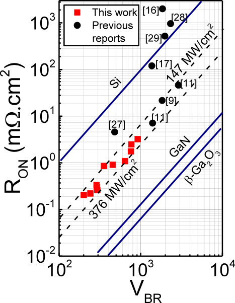
Figure 2: Benchmark plot against previous β-Ga2O3 lateral transistor reports.
The researchers comment: “The extreme-k field management strategy using BaTiO3 as the gate dielectric has thus resulted in superior performance even in the absence of additional field termination structures like field plates.”
The team hopes that future devices could include such termination to further improve performance.
https://doi.org/10.1109/TED.2020.3037271
The author Mike Cooke is a freelance technology journalist who has worked in the semiconductor and advanced technology sectors since 1997.


