


News: Microelectronics
2 December 2020
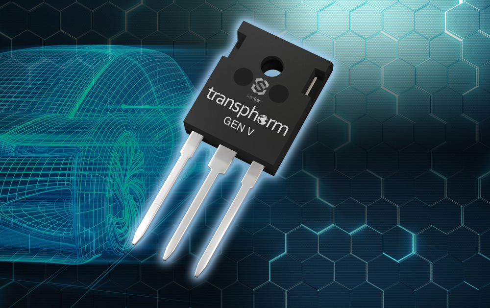
Transphorm sampling first Gen V FET under SuperGaN brand
Transphorm Inc of Goleta, near Santa Barbara, CA, USA — which designs and manufactures JEDEC- and AEC-Q101-qualified 650V and 900V gallium nitride (GaN) field-effect transistors (FETs) for high-voltage power conversion applications — is sampling its first Gen V device under its proprietary SuperGaN brand.
The TP65H015G5WS targets the electric vehicle (EV) market and provides what are claimed to be industry-leading performance enhancements, ease of designability, and optimized cost structure that is inherent to the SuperGaN device family. The firm claims that its Gen V GaN solution offers the lowest packaged on-resistance and delivers a 25% lower power loss over silicon carbide (SiC) in a standard TO-247-3 package, strengthening the potential of GaN in the EV power conversion market.
In March, automotive supplier Marelli announced a strategic partnership with Transphorm to collaborate on new GaN-based automotive/EV power conversion solutions, including on-board chargers (OBCs), DC-DC converters and powertrain inverters for electric and hybrid vehicles.
“Transphorm’s demonstration of achieving 10kW of power from a discrete packaged GaN device in a bridge configuration is further validation of the exciting promise of GaN for electric vehicle converters and inverters,” comments Dr Joachim Fetzer, CEO, Electric Powertrain Marelli. “As part of our previously announced partnership, we will continue to evaluate Transphorm’s industry-leading GaN devices and work together in support of a multi-year EV systems product roadmap,” he adds.
“We continue to innovate Transphorm’s SuperGaN FET technology, now offering the world’s lowest on-resistance in a standard TO-247-3 package in the market, targeted for electric vehicles and other higher-power conversion applications,” says Transphorm’s COO & co-founder Primit Parikh. “This allows customers to drive into double-digit kilowatts with a single device, continuing to demonstrate GaN’s ability to provide higher performance, lower system cost and higher power density,” he adds. “Our Gen V GaN platform is creating new design opportunities for power levels that previously required paralleling, while still offering the greater than 99% efficiency.”
SuperGaN technology outperforms silicon carbide
The SuperGaN Gen V platform incorporates all the learnings from its Gen IV predecessor: patented reduced packaging inductance technology, ease of designability and drivability (Vth of 4V for noise immunity), and gate robustness of +/-20Vmax, along with a simplified and reduced assembly structure. In an article published in EEWorld (‘Pushing the Boundaries of High Voltage GaN Power Conversion’) the TP65H015G5WS was compared to a similar on-resistance leading-edge SiC MOSFET in a standard TO-247-3 package. The devices were both operated up to 12kW at 70kHz in a half-bridge synchronous boost converter, resulting in Transphorm’s GaN device demonstrating up to 25% lower losses.
Transphorm has begun sampling the SuperGaN Gen V FET, a 15mΩ 650V device, which is unavailable with existing single-chip E-mode GaN technology due to its gate sensitivity, says the firm. Matching the lowest R available from typical SiC MOSFETs in a discrete package, the solution is capable of driving more than 10kW depending on the target application, such as EV OBCs and powertrain inverters, power supplies for rack-powered data-center servers, uninterruptible industrial power applications, and renewable photovoltaic inverters. The TP65H015G5WS will also be available for die-level module solutions that enable further paralleling for even higher power.
The firm anticipates its Gen V FET device to receive JEDEC qualification in mid-2021, with AEC-Q101 qualification expected thereafter.
Marelli partners with Transphorm


