


News: Optoelectronics
27 February 2020
III-V photodetectors integrated with silicon-on-insulator transistors
Researchers based in Korea have monolithically integrated indium gallium arsenide (InGaAs) photodiodes (PD) with silicon-on-insulator (SOI) metal-oxide-semiconductor field-effect transistors (MOSFETs) [Dae-Myeong Geum et al, IEEE Electron Device Letters, published online 17 January 2020].
The researchers from Korea Advanced Institute of Science and Technology (KAIST), Korea Institute of Science and Technology (KIST) and Hanyang University see the advantage from their monolithic three-dimensional (M3D) process as arising from the maturity of the InGaAs material process knowledge, compared with more recent laboratory work on devices using carbon nanotubes, transition-metal dichalcogenides, and so on.
In particular, “III-V materials can respond to the very long-wavelength region (VLWIR) not only visible and [short-wavelength] SWIR using [antimonide] Sb-based materials and type-II band alignment structures,” the team contends. They see their work as an important step for future high-resolution multi-color imagers. Such devices could find application in self-driving automobiles, time-of-flight sensing, and industrial surveillance. The photodiode/MOSFET combination should allow implementation of read-out integrated circuits (ROICs) on top of image signal processor (ISP) layers, creating more compact 3D devices (Figure 1).
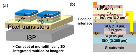
Figure 1: (a) M3D integrated high-resolution multi-color imager system concept. (b) Schematic of fabricated InGaAs photodiodes on SOI MOSFETs.
The SOI section used a 365nm silicon dioxide (SiO2) insulation layer. The MOSFET gate stack was built from hafnium aluminium oxide (HfAlOx) insulator and titanium nitride (TiN) electrodes. The structure was covered with sputtered SiO2 interlayer dielectric.
The surface was planarized using chemical mechanical polishing (CMP), before deposition of 40nm Al2O3 as bonding material. The InGaAs photodiode epitaxial material was also prepared for bonding with 40nm Al2O3 deposition. The Al2O3 surfaces were activated with oxygen plasma treatment to enable bonding.
The indium phosphide (InP) substrate was removed from the InGaAs photodiode material before formation of the photodiode electrodes and mesas/pixels. The top p+-InP contact was platinum/titanium/platinum/gold (Pt/Ti/Pt/Au). The bottom n+-InGaAs contact consisted of palladium/germanium/gold. Finally, connection was made between the photodiode cathode (n+-InGaAs) and the SOI MOSFET source terminal.
The reported process was carried out at room temperature, although the team reports that previous similar processing at 350°C resulted in “no degradation” in performance. In the present case, it was found that the performance of a 9μm-gate-length MOSFET was little changed by the bonding and photodiode fabrication processes, in terms of drain current and subthreshold swing.
The InGaAs photodiode demonstrated a forward/reverse ±1.5V bias dark current ratio of 104. The device showed a clear response under reverse bias when illuminated by 10.4μW 1550nm laser light. Shorter wavelengths in the range 785-980nm also showed a reasonable linear response. The response for 1500nm was stronger (0.7A/W) due to it being close to the band edge of the InGaAs material. Fitting with power-law current-power relations also suggested linear behavior with near-unity exponents. The fitted exponent of the illumination power was 0.97 for 1550nm light – the deviation from unity, the researchers suggest, could be explained by the presence of defects.
The external quantum efficiency (EQE) was 60% under 1550nm illumination. The value is declared to be “quite good”, considering that there was no anti-reflection coating. The team says that the performance was comparable to conventional InGaAs photodiodes.
The MOSFET- photodiode combinations were wired together into typical ROIC configurations (Figure 2): direct injection (DI) and source follower per detector (SFD). The team explains: “While photo-generated carriers are directly injected via the source on the output stage in the DI method, SFD uses the integration of photo-generated carriers in a capacitor during a specific period.”
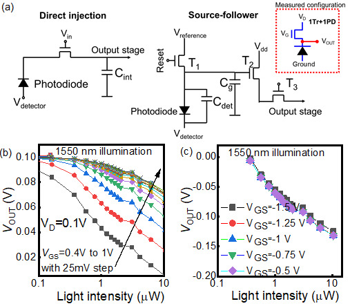
Figure 2: (a) Unit cell architectures of readout circuits and measuring devices as shown in inset. (b) Electrical response for DI operation (c) Electrical response for SFD operation.
With the drain at 0.1V bias, the gate potential was varied between 0.425V, subthreshold, and 1V under 1550nm illumination (Figure 2). Negative gate potentials between -0.5V and -1.5V, related to SFD operation, had little effect on the device response.
InGaAs photodiodes InGaAS Silicon-on-insulator MOSFETs MOSFETs
https://doi.org/10.1109/LED.2020.2966986
The author Mike Cooke is a freelance technology journalist who has worked in the semiconductor and advanced technology sectors since 1997.


