


News: Suppliers
20 July 2020
EVG completes construction of Cleanroom V building
EV Group – a supplier of wafer bonding and lithography equipment for semiconductor, micro-electro-mechanical systems (MEMS) and nanotechnology applications – has completed construction of its new Cleanroom V building, which nearly doubles cleanroom capacity at its corporate headquarters in St Florian, Austria, and will be used for product and process development, equipment demonstrations, prototyping and pilot-line production services. The Cleanroom V building, which is part of a €30m investment announced last year, will officially open in August.
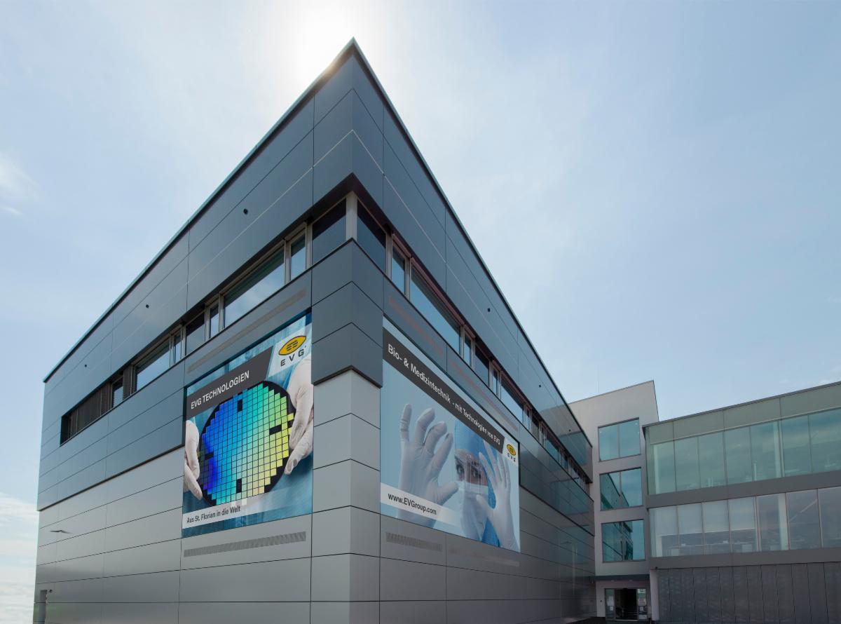
Picture: The new Cleanroom V facility nearly doubles cleanroom capacity at EVG's headquarters and houses a modern training center with multiple dedicated areas for customer and field engineer training.
The new Cleanroom V building is directly connected to EVG’s existing cleanroom and applications lab, and provides about 620m2 of additional Class 10 cleanroom floor space. The new building also houses a modern training center with multiple dedicated areas for training customers and field service engineers on EVG equipment platforms. As part of the expansion investment, the existing cleanroom and applications lab facility have also been upgraded, including the creation of redundant systems to ensure the highest availability and new safety features.
Enhancing centers of technology excellence
The added capacity afforded by the new Cleanroom V building will strengthen the capabilities of EVG’s NILPhotonics Competence Center and Heterogeneous Integration Competence Center, which provide process development services, and serve as open-access innovation incubators for customers and partners across the microelectronics supply chain. EVG says that, through these centers of technology excellence, it helps customers to accelerate technology development, minimize risk and develop differentiating technologies and products through the implementation of nanoimprint lithography and heterogeneous integration, respectively, while guaranteeing the highest IP protection standards that are required for working on pre-release products.
The new cleanroom is “arguably on par with some of the most technically advanced cleanrooms in Europe,” says corporate technology development & IP director Markus Wimplinger. “This new facility will greatly enhance our ability to co-develop future applications and technologies with our customers,” he adds. “In particular, we see it benefiting our competence centers, which have seen particularly strong activity and demand. The unique services offered at our NILPhotonics and Heterogeneous Integration Competence Centers enable our customers and partners to shorten development cycles and create novel products in these critical application areas.”
EVG reckons that, with its technology competence centers and strong customer partnerships, it is uniquely positioned to provide uninterrupted process development services and support for its customers. At the same time, its local installation and support teams as well as remote support capabilities enable continuous installation and service operations of EVG’s equipment.


