


News: LEDs
30 July 2020
First claim of nitrogen-polar III-nitride tunnel-junction light-emitting diodes
Researchers based in China and Saudi Arabia claim the first demonstration of nitrogen-polar tunnel-junction (TJ) indium gallium nitride (InGaN) light-emitting diodes (LEDs) [Yuantao Zhang et al, ACS Photonics, published online 28 May 2020]. N-polar tunnel junctions with good performance have previously been reported, but up to now only III-polar III-nitride TJ-LEDs have been achieved, according to the researchers.
The team from Jilin University in Changchun, China, King Abdullah University of Science and Technology (KAUST) in Saudi Arabia, China’s Institute of Semiconductors, and Zhengzhou University used polarization-doped aluminium gallium nitride (AlGaN) to enhance the performance of the TJ, giving a higher hole concentration and boosting lateral current spreading from the electrodes.
Despite being the first N-polar TJ-LED report, the researchers admit: “The current density of the tunnel junction in this work is still lower than those of the reported N-polar GaN/InGaN/GaN TJs, which may be caused by the use of Al-rich AlGaN for the tunnel junction, though it could be improved by further optimization.”
The team adds: “It is worth mentioning that the proposed tunnel junction in this work can be applied to other spectral ranges, not only UVB and UVC, but also longer-wavelength yellow and red with modifications of material and structural parameters.”
The N-polar III-nitride material (Figure 1) was grown by metal-organic vapor phase epitaxy on c-plane sapphire.
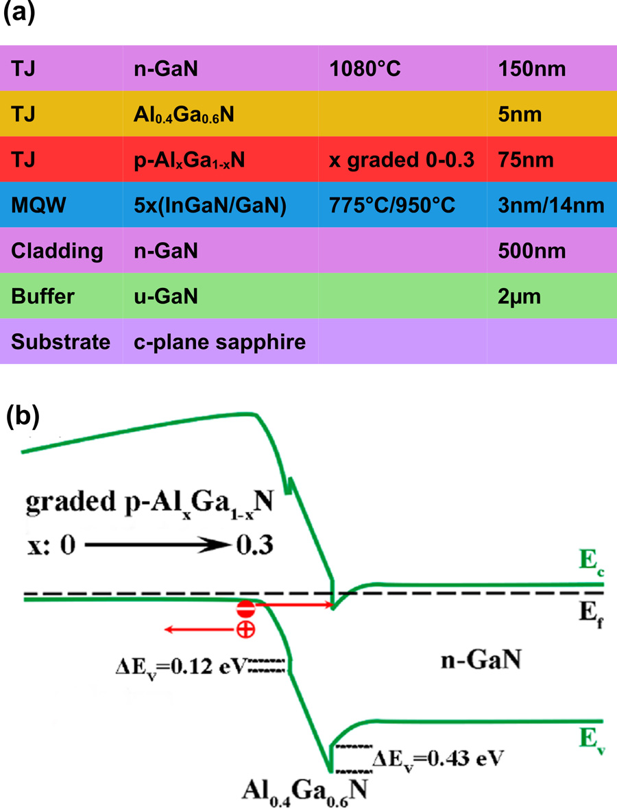
Figure 1: (a) Epitaxial layers of TJ-LED, and (b) sketch of expected energy-band diagram in tunnel-junction region.
The top n-GaN layer of the tunnel junction was optimized using periodic delta-doping with silicon sourced from silane (SiH4). This avoided the appearance of ‘dots’ on the surface of the material, as occurred when the siliane was supplied continuously. Also, in continuous growth, undulations were seen, attributed to step-bunched growth. Closer study of the dots showed them to be V-pits, which degrade device performance by offering current leakage paths.
The periodic doping was carried out with continuous ammonia (NH3) flow and alternate bursts of silane and trimethyl-gallium (TMG). Each period was preceded by a 5-second purge without silane or TMG. The researchers describe the resulting material as being effectively a “periodic superlattice comprising unintentionally doped u-GaN and SiNx layers”.
The team comments: “We speculate that the suppressed formation of V-pits may be related to the reduced tensile stress amid the periodic Si-delta doping as compared to the conventional continuous Si doping in N-polar GaN.”
The researchers optimized the period thickness and silane flow rate. With 20nm thickness and 16nmol/min flow, the n-GaN layer was found to have an electron concentration and mobility of 2x10¹⁸/cm3 and 329cm2/V-s, respectively.
The other component of the tunnel junction – the underlying p-AlGaN layer – was kept to a relatively thin 75nm in order to optimize the polarization-doping effect of the graded composition. The magnesium p-type dopant was supplied by bis-cyclopentadienyl magnesium (Cp2Mg). The hole concentration and mobility were 9x10¹⁷/cm3 and 7.5cm2/V-s, respectively. A thin Al0.4Ga0.6N interlayer was placed between the p- and n-type layers of the tunnel junction.
The material was fabricated into 250μmx250μm mesa-type LEDs. The contact metal to the n-GaN of the tunnel junction and the n-side of the device consisted of titanium/aluminium/titanium/gold. A reference LED, with the top n-GaN layer of the tunnel junction replaced by 3nm p-Al0.3Ga0.7N, used a nickel/gold p-contact.
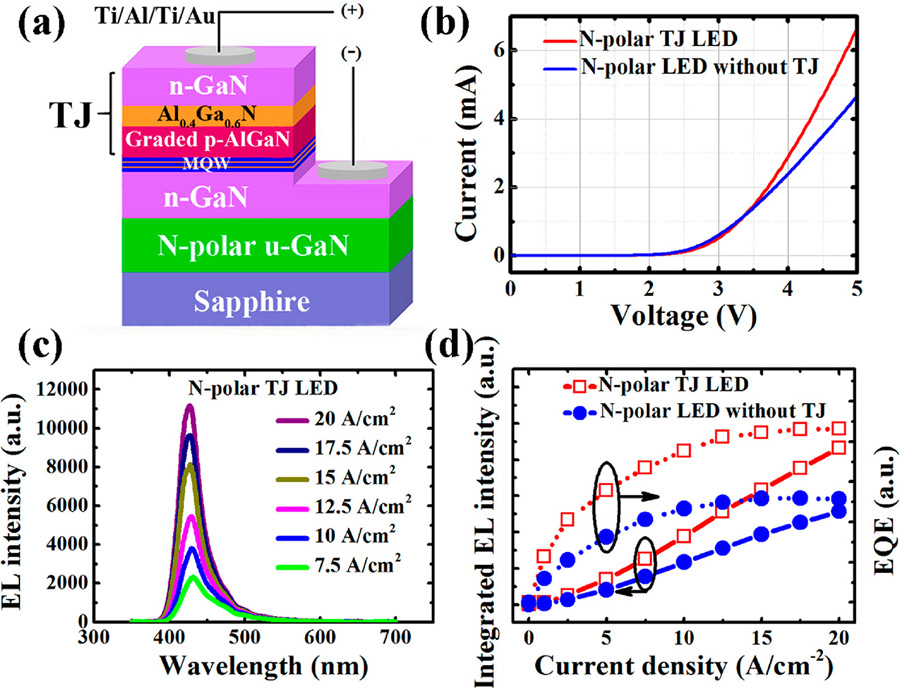
Figure 2: (a) Schematic diagram of TJ LED under electroluminescence (EL) operation. (b) Current-voltage curves of tunnel-junction and reference LEDs. (c) EL spectra of TJ LED under varying current density. (d) Integrated EL intensity and relative EQE of tunnel-junction and reference LEDs versus current density.
The tunnel junction enabled a higher current for a given forward voltage to be achieved (Figure 2). The turn-on voltage of both devices was about 2.5V. In the linear region, the total resistance was 264Ω with the tunnel junction and 439Ω in the reference device. The peak wavelength of both devices was ~430nm.
In terms of light output, the TJ-LED delivers increasing intensity over the reference above 2A/cm2 injection current density. By 20A/cm2 injection, the TJ-LED’s light output was 70% more intense. The external quantum efficiency (EQE) was also higher – 1.7x at 20A/cm2. The researchers attribute the improved performance to the lower total resistance of the TJ-LED.
https://dx.doi.org/10.1021/acsphotonics.0c00269
The author Mike Cooke is a freelance technology journalist who has worked in the semiconductor and advanced technology sectors since 1997.


