


News: Microelectronics
23 July 2020
ALLOS transferring RF & power electronics patents & know-how to new GaN-on-Si entrant Azur Space
On 8 July, IP licensing & technology engineering firm ALLOS Semiconductors GmbH of Dresden, Germany disclosed a deal to sell its gallium nitride (GaN) RF and power electronics business to Azur Space Solar Power GmbH of Heilbronn, Germany, which develops and produces multi-junction solar cells, with a view to focusing on its GaN-on-silicon micro-LED epiwafer technology for up to 300mm.
Patent analysis and technology intelligence firm Knowmade notes that Azur Space is a new entrant in the power electronics business, with no pre-existing intellectual property assets related to GaN-on-Si epitaxy and power GaN device technology, but it does have the ability to leverage its manufacturing expertise and facilities for high-volume production with a relatively limited initial investment (€10m).
Since its foundation in 2014, ALLOS has made its epiwafer technology – inherited from Azzurro Semiconductors – available through licensing and technology transfer to “high-power electronics companies that would like to enter the GaN-on-Si sector and avoid the cost, risk and uncertainty of starting their own epi development from scratch”. In other words, ALLOS would enable new players to safely enter the GaN-on-Si business, relying on its patented and proprietary growth techniques and epi-structures.
In 2017, the licensing & technology engineering firm further strengthened its value proposition by disclosing a carbon-doping-free GaN-on-Si technology, offering good dynamic resistance, good crystal quality and extremely low leakage current all at once, enabling customers to overcome the usual trade-off between these parameters when using carbon doping in epi-structures. Moreover, it would provide an effective way for customers to avoid conflicts with well-established IP competitors relying on carbon doping to achieve the power electronics industry’s requirements. As of 2017, ALLOS’ approach was based on the insertion of multiple interlayers in an unintentionally doped thick GaN buffer layer (Figure 1). Knowmade says that, to its knowledge, neither ALLOS nor Azzurro has filed patents describing such a structure, or how to design and grow the interlayers in order to effectively reduce the leakage current in high-voltage applications.
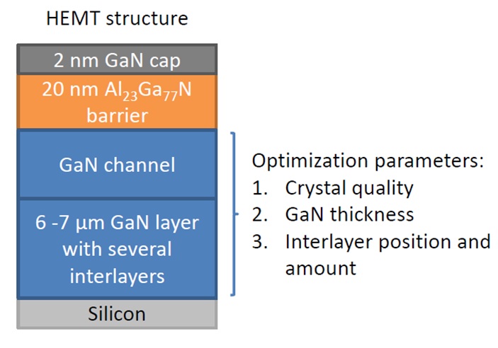
Figure 1: Typical GaN-HEMT epi-structures grown by MOCVD without intentional carbon doping or other doping. Electrical performance is optimized by position and number of interlayers. Source: ‘Low vertical leakage current of 0.07µm/mm2 at 600V without intentional doping for 7µm-thick GaN-on-Si’ presented at ICNS-12 in Strasbourg, France (July 2017).
At the time of Azzurro’s bankruptcy, the GaN-on-Si epi-foundry had filed 29 patent families (i.e. single inventions patented in multiple countries). Most of them were reviewed by Knowmade in the ‘GaN-on-Silicon Patent Landscape 2020’. However, since ALLOS was created in 2014 and acquired Azzurro’s technology, know-how and patents, the engineering and consulting company has not relied on patents to protect new inventions. As a result, ALLOS’ IP portfolio has shrunk to eight alive patent families (21 of Azzurro’s inventions were abandoned and no patent application has been filed by ALLOS), grouping less than 50 patents and patent applications filed in the main area of interest for Azzurro’s business: Europe (12), USA (9), China (8), Korea (5), Japan (2) and Taiwan (2). Furthermore, as of 2020, all of ALLOS’ live patent families have already been the subject of a transfer of rights to Azur Space.
Indeed, the first patent transfers between the two companies occurred in 2015 and concerned the most relevant inventions for power applications, filed by Azzurro in 2013:
- ‘P-doping of group-III-nitride buffer layer structure on a hetero-substrate’, to provide good stress management and the high resistivity required for RF & power applications (US Patent 9,496,349);
- ‘Layer structure for a group-III nitride normally-off transistor’, with a recess-free design (US Patent 9,773,896).
Both patent families were granted thereafter with protection in main market areas such as Europe, USA, China and Korea, with the notable exception of Japan. Moreover, four domestic granted patents (filed only in Germany), dealing with electronics as well as optoelectronics, were transferred to Azur Space in 2016:
- ‘III-nitride p-channel transistor structures to produce logic components comprises growing an aluminum indium nitride barrier layer on a group-III nitride buffer layer’ (patent DE10200403434);
- ‘Field-effect transistors, comprises an aluminum-gallium-indium-nitrogen layer, aluminum-gallium-nitrogen intermediate layer, and another aluminum-gallium-indium-nitrogen layer’ (patent DE102006030305);
- ‘Group-III nitride transistor component on a Si substrate for high temperature and microwaves, with a buffer layer formed by gas phase epitaxy’, iron-doping of GaN-based buffer layers (patent DE10256911);
- ‘Production of a planar tear-free light emitter structure comprises applying an aluminum-containing group III-V seed layer, aluminum-containing group III-V intermediate layers, and silicon nitride intermediate layers on a Si substrate’ (patent DE10151092).
Eventually, ALLOS completed the IP transfer in second-quarter 2020 with two additional patent families related to improvements in terms of stress management when using a masking layer (e.g. SiN) for the growth of high-quality GaN epilayers on silicon substrates, especially for LED applications (EP patent 2,112,699 and US patent 9,406,505).
Interestingly, in 2019 Azur Space also acquired IP rights on two patent families filed by the Ulm University spin-off MicroGaN related to a diode circuit combining a GaN high-electron-mobility transistor (HEMT) and a GaN Schottky barrier diode (EP patent 2,633,555) including a GaN-on-Si embodiment, and a method of contacting a number of GaN devices together in a more compact way (US patent 8,748,944).
In conclusion, the present deal provides Azur Space with very relevant patents to develop GaN-on-Si technology and stand out from competitors, assesses Knowmade. Besides patents, it can rely on ALLOS’ experise in the field, although not all aspects of ALLOS’ technology are visible in patents. Indeed, the company seems to have put the emphasis on know-how and technology transfer rather than IP licensing in the development of its business. In fact, ALLOS is actively developing its GaN-on-Si technology for micro-LEDs and, according to the latest announcement, will focus its activities on micro-LEDs in the coming years. However, this has not yet translated into patenting activity, so it is likely to follow the same strategy as for power & RF electronics, focusing on trade secrets and technology transfer.
The power GaN patent landscape and GaN-on-Si patent landscape have been evolving rapidly in recent years, notes Knowmade, with numerous innovative startups and major power electronics’ players aiming to strengthen their position, to prepare for the promising power GaN markets. For any of them, GaN-on-Si IP is crucial and has fostered multiple acquisitions and partnerships with well-established players in the field. In this very dynamic environment, Knowmade has set up a GaN Power & RF Patent Monitor service to track and analyze, month by month, the latest patenting activity of IP competitors engaged in the development of these technologies.
GaN-on-Si firm ALLOS sells high-power electronics and RF business to AZUR


