


News: Microelectronics
3 July 2020
Improving aluminium nitride nucleation and regrowth on sapphire
Researchers in China and Taiwan have been seeking ways to improve the growth quality of aluminium nitride (AlN) on sapphire with a view to power electronics applications [Xianfeng Ni et al, IEEE Transactions on Electron Devices, published online 29 May 2020].
To take advantage of the enhanced critical electrical field of ultra-wide-bandgap AlN, it is vital to reduce potential leakage through crystal defects. Presently, the quality of AlN templates is relatively poor, with threading dislocation densities of the order 108-1010/cm2.
The team from Southeast University Suzhou Campus in China, Suzhou Hanhua Semiconductor Inc in China, and Lextar Electronics Corp in Taiwan used ~1700°C high-temperature annealing after nucleation growth to significantly improve crystal quality of AlN/sapphire templates.
“The demonstrated method paves a way for producing high-quality low-cost AlN templates for use of power electronics production,” the researchers write.
Apart from the high critical field before electrical breakdown, AlN also has a high thermal conductivity, which would enable improved thermal management in power diodes, transistors and more complex integrated circuits.
The high critical field could lead to much faster, more energy-efficient and more compact power switching devices, compared with devices based on silicon, gallium nitride or silicon carbide.
AlN is also an attractive substrate for aluminium gallium nitride structures needed for deep-ultraviolet-emitting devices, with applications such as sterilization and water purification.
The researchers grew 300nm AlN nucleation layers on 2inch-diameter sapphire substrates, using metal-organic chemical vapor deposition (MOCVD). The precursors for the Al and N components were trimethyl-aluminium and ammonia (NH3), respectively. The samples were loaded into an annealing furnace in pairs, with the AlN surfaces facing each other. The annealing temperature was variously in the range 1670-1730°C. The treatment was carried out in a nitrogen atmosphere at 500Torr pressure.
The annealing process halved the full-width at half maximum (FWHM) of the (002) x-ray diffraction peak from 130arcsec down to 61.9 arcsec for the 1700°C treatment. The results for 1670° and 1730°C were 64.2arcsec and 62.5arcsec, respectively.
The reduction of the (102) peak was even more dramatic: 1610.5arcsec, as-grown (i.e. without annealing), down to 383.1arcsec, 350.7arcsec and 344.8arcsec for 1670°C, 1700°C and 1730°C annealing, respectively. The (102) peak is seen as being sensitive to mixed or edge-type crystal fault structures such as threading dislocations.
After the annealing, the samples were subjected to further 1200°C AlN regrowth, resulting in 1-2μm layers. The nitrogen/aluminium ratio during the regrowth process was 150, i.e. nitrogen-rich.
The (002) x-ray diffraction peak was increased by regrowth in all the samples. The as-grown sample FWHM for the peak after 2μm regrowth was 174arcsec. By contrast, the (102) peak FWHM tended to decrease with regrowth, most noticeably with the as-grown sample reducing to around 534arcsec. The 1730°C annealing resulted in a (102) peak FWHM of 255arcsec after regrowth.
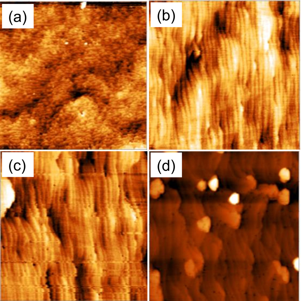
Figure 1: 5μmx5μm AFM images for as-grown (a) and annealed AlN at 1670°CC (b), 1700°C (c) and 1730°C (d).
Surface inspection using atomic force microscopy (AFM) showed the annealed samples having more pronounced atomic steps (Figure 1). Such steps can improve regrowth processes. The root mean square (RMS) roughness values for as-grown and 1670°C-1730°C annealing were, in order of increasing temperature, 0.74nm, 0.27nm, 0.32nm and 1.4nm.
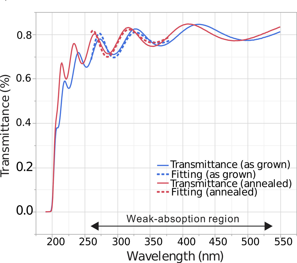
Figure 2: Transmittance data for as-grown and 1700°C annealed AlN nucleation samples.
The transmission of electromagnetic radiation by the samples was measured in the wavelength range 200-550nm, covering from the deep-ultraviolet (UV) and visible light out to the green part of the spectrum (Figure 2).
In the 260-270nm deep-UV portion, the annealed samples demonstrated 3-4% more transmission than the as-grown samples. The team comments: “The slight improvement could be due to the recrystallization of AlN upon annealing, leading to better transmittance.”
The undulation of the curves is attributed to interference fringes from the multiple reflections/transmissions of the interfaces in the samples.
https://doi.org/10.1109/TED.2020.2991397
The author Mike Cooke is a freelance technology journalist who has worked in the semiconductor and advanced technology sectors since 1997.


