


News: LEDs
26 June 2020
Carrier-localization engineering for deep-ultraviolet light-emitting diodes
China’s Peking University has used deep-ultraviolet (DUV, <300nm wavelength) light-emitting ‘self-assembled sidewall quantum well (SQW)’ structures to improve light output power performance of diodes based on aluminium gallium nitride (AlGaN) compound semiconductor alloys [Y. H. Sun et al, Appl. Phys. Lett., vol116, p212102, 2020].
The sidewall structures arose from bunching effects during multiple quantum well (MQW) material growth processing on (0001) c-plane sapphire substrates with different miscut angles. [One should stress here that the SQW abbreviation for ‘sidewall quantum well’ is non-standard; more normally, SQW is used for ‘single quantum well’.]
Potential applications for DUV light-emitting diodes (LEDs) include water/air purification, non-line-of-sight communication, biological/chemical analysis, ultraviolet curing, environmental sensing, and plant growth lighting. Present DUV LEDs, however, suffer from poor efficiency and low light output power performance. These problems are related to defects in the materials used in such devices.
One approach to improved performance would be to increase material quality by using AlN substrates to enable closer lattice matching with AlGaN heterostructures, compared with sapphire. However, AlN substrates of appropriate quality, size and cost have yet to be developed.
The Beijing researchers see their SQW approach as being a potential “subversive framework” that involves “an active region structure with low sensitivity to the density of defects to reduce the tough requirements on the quality of AlN and AlGaN”. An additional factor is that the SQW structures create carrier localization effects that can improve recombination into photons, and avoid carriers being trapped by dislocations and then transitioning to the ground state with no light emitted.
The material was grown on miscut (0001) c-plane sapphire using metal-organic chemical vapor deposition (MOCVD). The precursors were trimethyl-gallium/aluminium and ammonia (NH3). The miscut angles, relative to the m-plane, were 0.2° (sample A), 2° (B), and 4° (C).
The nucleation layer was 20nm 930°C AlN. The main 1μm AlN template layer was grown at 1250°C. Further 1250°C growth consisted of a 0.5μm AlN/Al0.55Ga0.45N superlattice, and 1.5μm silicon-doped n-Al0.55Ga0.45N as the electron source/n-contact.
The temperature was then reduced to 1070°C for the final 10-period MQW structure of 2.3nm/10nm Al0.37Ga0.63N/Al0.5Ga0.5N pairs.
Atomic force microscopy (AFM) showed an increased surface roughness as the miscut angle increased: 0.71nm root mean square (RMS) for sample A, and 3.85nm and 6.3nm for samples B and C, respectively. The increased angle also increased the density of macrostep bunches.
Based on cross-sectional high-angle annular dark-field scanning transmission electron microscopy (HAADF-STEM) and energy dispersive spectroscopy (EDS) analysis, the researchers give an average terrace widths for samples B and C of 320nm and 200nm, respectively (Figure 1). The narrower terraces of sample C reflect the higher density of macrostep bunches. The step heights were 14nm for sample B and 22nm for C.
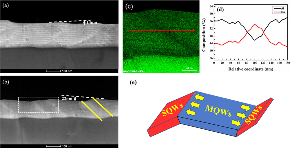
Figure 1: Cross-sectional HAADF-STEM images of sample B (a) and sample C (b), and EDS mapping of selected area in sample C (c), (Al composition shown by green intensity); (d) relative Al and Ga compositions along horizontal red arrow in (c); (e) schematic images of exciton movement in MQW and SQW regions.
The EDS mapping showed ~10% reduced Al content in the regions of the steps. The researchers explain this as being due to the higher surface mobility of Ga relative to Al in the growth process. The reduced Al means that the effective bandgap will be reduced in the step area, attracting free carriers and creating localization. Such effects can lead to increased recombination into photons, relative to non-radiative dissipation of the input power.
Cathodoluminescence (CL) on a sample with 0.5° miscut substrate suggested that the bandgap in the step region was such as to produce a spectral peak around 293nm wavelength, compared with 280nm from the smooth terraces. The longer wavelength at the step suggest a narrower bandgap. The relatively small miscut angle of 0.5° was used due to experimental limitations of the CL technique.
Temperature-dependent photoluminescence (TDPL) also showed two spectral peaks with the shorter wavelength associated to the smooth MQW terraces and the longer wavelength to the SQW step regions, in accordance with the CL study.
The internal quantum efficiency (IQE) was assessed by comparing the room-temperature and 10K PL intensities. The intensity at 10K was assumed to result from 100% IQE. For samples A-C, the room-temperature IQE was determined at 46%, 54% and 59%, respectively. By separating the behaviors of the SQW and MQW emissions using Lorentz curve fits, the IQE of the SQW region of sample B was estimated to be 56%, while the MQWs only managed 45.6%.
X-ray analysis of MQWs grown directly on the AlN template layer suggested threading dislocation densities (TDD) of 1.56x10¹⁰/cm2, 1.17x10¹⁰/cm2 and 6.4x10⁹/cm2 for substrate miscut angles of 0.2°, 2° and 4°, respectively. While the density was much reduced for the 4° sample, these are all relatively high values. The researchers see the lower TDD value for the 4° MQW structure as “a main factor contributing to the increase in IQE”.
The team adds: “Another factor accounting for the increased IQE is the effect of the additional one-dimensional carrier confinement, resulting in much stronger localization of carriers to avoid interactions with TDs.”
Time-resolved PL was used to determine fluorescence lifetimes: 126ps for sample A and 508ps for C. Sample B was studied more closely, separating the MQW and SQW parts: 155.9ps and 208.9ps, respectively. “These results show that the fluorescence lifetime of the SQWs is significantly prolonged than that of MQWs, indicating that the non-radiative recombination in SQWs is more effectively suppressed compared to the case of MQWs,” the team explains.
DUV LEDs were produced on 0.2° and 2° miscut substrate materials. The 4° miscut material was found to have problems with electrical leakage effects arising from the large surface fluctuations.
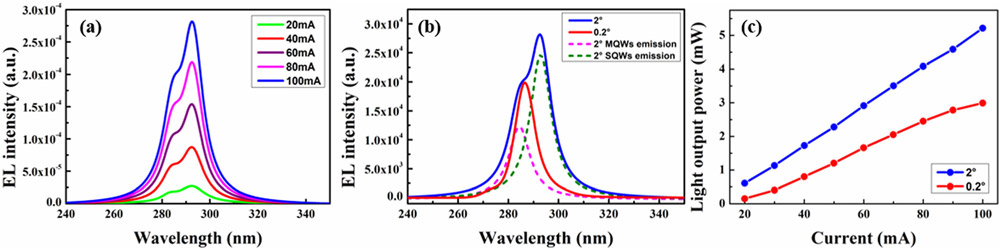
Figure 2: (a) EL spectra of DUV-LED on 2°-miscut sapphire at different currents; (b) EL spectra from DUV-LEDs with miscut angles of 0.2° and 2° at 100mA injection; (c) LOP at different injection currents.
The 2° ‘SQW sample’ was found to have a double, overlapping peak spectrum (Figure 2). The light output power (LOP) was 5.1mW with 100mA injection, compared with 2.99mW for the ‘MQW sample’ with 0.2° miscut substrate.
Again separating the ‘SQW sample’ into SQW and MQW components, the researchers found the intensity of the SQW emission to be greater than from the MQW emission from the 0.2° ‘MQW sample’, while the MQW component was less intense. The researchers point out that the effective emission area of the MQW component was restricted by the presence of SQW structures. The wavelengths of both peaks in the SQW sample were shorter than 300nm, putting them in the ‘DUV’ range.
The researchers comment: “These results further verify that the proposed active region involving SQWs has much greater potential in device performance than that with only MQWs, especially when the material quality of AlN and AlGaN remains at a poor or medium level.”
https://doi.org/10.1063/5.0008339
The author Mike Cooke is a freelance technology journalist who has worked in the semiconductor and advanced technology sectors since 1997.


