


News: Microelectronics
4 March 2020
Growing ε polytype gallium oxide with gallium nitride
Researchers based in Germany and Italy have been exploring the growth of ε-polytype gallium oxide (ε-Ga2O3) combined with gallium nitride (GaN) on sapphire substrates with a view to deployment in high-electron-mobility transistors (HEMTs) [Stefano Leone et al, Journal of Crystal Growth, vol534, p125511, 2020].
GaN-based high-frequency and high-voltage power devices are moving to wider commercial deployment in AC-DC inverters, power supplies, 600V switches, and the generation of communications and radar radio signals. The combination of GaN with ferroelectric ε-Ga2O3 could lead to interesting further electronic opportunities.
The ε-Ga2O3 material also has a strong spontaneous charge polarization, arising from the crystal structure and stronger ionic character of the chemical bond. Such polarization could give rise to two-dimensional electron gas (2DEG) HEMT channels with very high carrier density. There are, of course, also strain-dependent piezoelectric effects to be expected.
Ferroelectricity has mainly been deployed in non-volatile memory devices up to now, but recent research has also used the property to create ‘negative capacitance’ gate stacks. Such negative capacitance enables the subthreshold swing to go lower than the standard thermal limit of 60mV/decade. Such sharply switching devices are of interest in silicon electronics for low-voltage operation and low power consumption. Of course, GaN-based electronics is not so interested in low voltage.
One factor that has to be considered is that the β polytype crystal structure is more stable and the ε form of Ga2O3 decomposes above 700°C. This restricts the thermal budget of processes involving the material.
The team from Fraunhofer Institute for Applied Solid State Physics (IAF) in Germany, University of Parma in Italy, Institute of Materials for Electronics and Magnetism (IMEM-CNR) in Italy and Albert-Ludwigs Universität Freiburg in Germany focused on growth using metal-organic chemical vapor deposition (MOCVD) since it is the technique most favored in manufacturing. The researchers claim that their work is the first investigation of GaN/ε-Ga2O3 MOCVD.
The team employed two separated MOCVD reactors for deposition of ε-Ga2O3 and GaN. The material surfaces were exposed to air on transfer between the chambers. The GaN deposition used trimethyl-gallium (TMGa) and ammonia (NH3) precursors in hydrogen carrier gas. The substrate was mainly on-axis sapphire: (001) aluminium oxide (Al2O3). The ε-Ga2O3 was deposited in a cold-wall system at 610°C. The precursors for this were TMGa and water (H2O) in hydrogen carrier gas.
The GaN growth rate at 1050°C was around 1µm/hour. The ε-Ga2O3 deposition was at about half that rate, 500nm/hour. Some samples included a 10nm silicon nitride (SiN) passivation layer for studying electronic properties towards the fabrication of HEMTs. The SiN was deposited using inductively coupled plasma CVD, using silane (SiH4) and NH3.
The ε Ga2O3 polytype has an orthorhombic (pseudo-hexagonal) crystal structure with nominal 8.8% lattice mismatch with GaN. The researchers also investigated depositing the ε-Ga2O3 before the GaN – the drawback being that ε-Ga2O3 begins a transition to β-Ga2O3 at 700°C, which completes at 900°C. Thus, with ε-Ga2O3-first deposition the researchers reduced the GaN growth temperature to 690°C. Although the GaN-on-ε-Ga2O3 (GaN/ε-Ga2O3) surface was smooth, there were several defects visible in microscopic inspection.
Depositing the GaN at high temperature (1050°C) converted the ε material to β. according to x-ray analysis. By contrast, the low-temperature GaN/ε-Ga2O3 remained in the ε phase. The crystal quality of the overlying GaN is described as “poor” in both cases, on the basis of large full-width at half-maximum (FWHM) values for various x-ray rocking curve peaks. The low-temperature sample was particularly poor.
Although the growth of ε-Ga2O3 on GaN was better, the deposition tended to begin with 3D islands that later began to coalesce. Such behavior could lead to decent quality in thick layers, but the researchers were more interested in creating thin ε-Ga2O3 on GaN heterostructures with a view to fabrication of HEMTs.
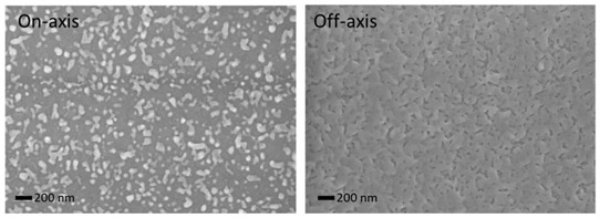
Figure 1: SEM studies of 5-minute ε-Ga2O3 MOCVD on (left) on-axis and (right) 4° off-cut GaN on sapphire.
To encourage 2D layer-by-layer growth of ε-Ga2O3 the team tried using 4° off-cut (0001) sapphire substrates, giving the GaN surface a step-and-terrace texture. “The coalescence in this sample seems to be much more effective than in the on-axis samples,” the researchers observe from scanning electron microscope (SEM) studies (Figure 1).
Capacitance-voltage (CV) analysis of the materials detected 2DEG behavior only when the sample was capped with SiN passivation. However, there was a high level of hysteresis in the curves, ~0.9V, suggesting the presence of defects or ionized states. A SiN/ε-Ga2O3/GaN structure was found to have a carrier density profile consistent with a combined SiN/ε-Ga2O3 barrier thickness of 25nm. The SiN passivation was 10nm.
The growth time of the ε-Ga2O3 was 17 minutes. Thinner layers with shorter growth times down to 3 minutes were less uniform and consequently performed less well in CV measurements. Difficulties in making Ohmic contacts has inhibited the performance of Hall measurements and hence the assessment of carrier mobility. Sheet resistance values were relatively high: 1300-2200Ω/square and 3300Ω/square for on- and off-axis samples, respectively.
The sheet carrier density was estimated to be 6.4x10¹²/cm2, using the CV data. This value was well short of theoretical expectations of 1.2x10¹⁴/cm2, using Schrödinger-Poisson modeling. The modeled values for AlN and Al0.25Ga0.75N barriers are 6.5x10¹³/cm2 and 1.1x10¹³/cm2, respectively. The higher expectation for ε-Ga2O3 barriers rests on a higher spontaneous charge polarization of the crystal structure and the more ionic character of the chemical bonds.
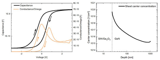
Figure 2: (left) Capacitance- and conductance/angular frequency (G/ω) versus voltage and (right) CV-derived carrier density versus depth profile.
The suppression of the 2DEG sheet carrier density in the experimental samples relative to theoretical expectations could be due to factors such as non-optimized morphology and high defect densities. Despite this, the team sees their results as being “very promising”. One key component in future HEMT development would be the fabrication of low-contact-resistance Ohmic source-drain electrodes without exceeding the 700°C thermal limit imposed by the ε-to-β polytype phase transition of the Ga2O3. The team points hopefully to recent work using titanium/gold annealed for three hours at 300°C, which gave low reported contact resistance on ε-Ga2O3.
Polytype gallium oxide GaN HEMTs TMGa MOCVD
https://doi.org/10.1016/j.jcrysgro.2020.125511
The author Mike Cooke is a freelance technology journalist who has worked in the semiconductor and advanced technology sectors since 1997.


