


News: Optoelectronics
1 May 2020
High-index-contrast gratings for III-nitride vertical-cavity surface-emitting laser diodes
Researchers based in Taiwan and Sweden claim the first demonstration of high-index-contrast grating (HCG) as the top mirror for III-nitride (III-N) vertical-cavity surface-emitting laser (VCSEL) diodes [Tsu-Chi Chang et al, ACS Photonics, published online 26 February 2020]. The team from National Chiao Tung University and Chalmers University of Technology hope that the development will lead to “substantial thickness reduction, polarization-pinning, and setting of the resonance wavelength by the grating parameters”.
The VCSEL used epitaxial III-N material flipped onto a silicon substrate. The epitaxial source material consisted of patterned sapphire substrate (PSS), gallium nitride (GaN) nucleation,2μm undoped GaN, 5μm n-GaN contact, 10 pairs of indium gallium nitride (In0.1Ga0.9N)/GaN (3nm/8nm) multiple quantum well (MQWs) for an active region, a 10nm p-type aluminium gallium nitride (Al0.2Ga0.8N) electron-blocking layer, and a 170nm p-GaN contact layer.
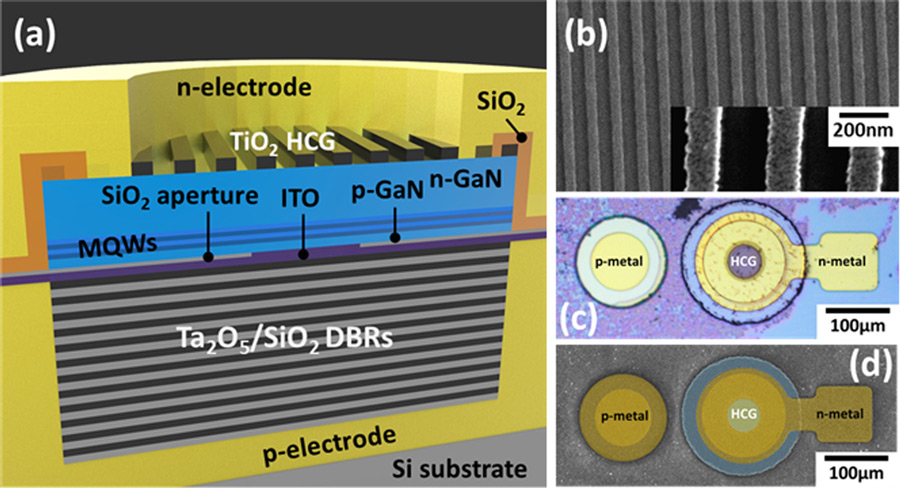
Figure 1: (a) Three-dimensional illustration of GaN VCSELs. (b) Top-view scanning electron microscope (SEM) image of TiO2 HCG. Top-view (c) optical microscopy and (d) SEM images of VCSELs.
VCSEL fabrication began with atomic layer deposition (ALD) of 30nm silicon dioxide (SiO2) on the p-GaN. A 10μm-diameter current aperture was opened before applying 10nm sputtered indium tin oxide (ITO) transparent conductor. The final part of the p-side of the device consisted of electron-beam evaporation of a distributed Bragg reflector (DBR) composed of 12-pairs of SiO2 and tantalum oxide (Ta2O5) dielectric layers. Typical GaN-based VCSELs use top and bottom DBRs.
The next stage of processing consisted of thermocompressive flip-chip bonding to a silicon substrate. Laser lift-off removed the sapphire substrate and further GaN material was also removed using chemical-mechanical polishing (CMP), giving a 5μm thickness with an n-GaN surface.
The HCG grating was fabricated using sputtering of titanium dioxide (TiO2) and SiO2, followed by lift-off patterning, using the SiO2 and nickel as hard masks. The etching used inductively coupled plasma reactive ions. The grating consisted of strips of TiO2 with 344.5nm pitch. The strip height and base width were 112.3nm and 177.8nm, respectively.
The device was completed with electrical isolation and deposition of the n- and p-contact metals.
The VCSEL was tested in pulsed mode with 0.1μs width and 0.3% duty cycle (Figure 2). The lasing threshold was 25mA, equivalent to 31.8kA/cm2 density. The turn-on voltage came at 6.9V. The researchers report: “Compared to our previously reported VCSELs with two dielectric DBRs, the HCG VCSEL (which has one of the DBRs replaced by an HCG) has a higher threshold current density, lower optical output power, and higher turn-on voltage.”
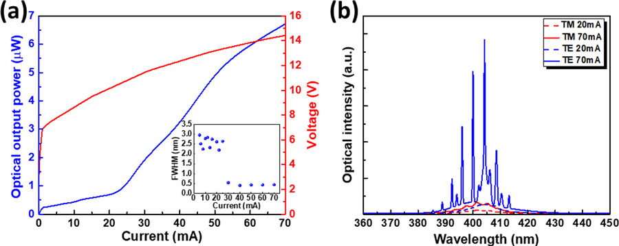
Figure 2: (a) Pulsed optical output power−current−voltage (L−I−V) characteristics of HCG GaN-based VCSEL. Inset: current-dependent line width. (b) Optical emission spectra in two orthogonal polarization directions with electric field parallel to grating bars (TE) and perpendicular to grating bars (TM) below and above threshold.
The team explains the worse performance of the HCG by the thicker n-GaN layer (~5μm) in the final device, compared with that of the previous DBR-only VCSEL (~940nm). The researchers believe that some unintentionally doped GaN may have remained after the CMP, further increasing the contact and series resistance. The thicker n-GaN also absorbs more photons, increasing the threshold current and reducing optical output power.
The laser output was strongly polarized transverse electric, parallel to the grating bars above threshold. The highest peak came at 404.2nm. From the spacings between the multi-mode peaks (~4.2nm), the researchers estimated the effective cavity length to be 5.1μm. The line-width of the modes reduced from 2.5nm to 0.5nm as the current passed through threshold.
The beam divergence with 60mA drive current was 10° full-width at half-maximum (FWHM).
VCSEL Silicon substrate Sapphire substrate GaN InGaN MQWs AlGaN ALD DBR
https://dx.doi.org/10.1021/acsphotonics.9b01636
The author Mike Cooke is a freelance technology journalist who has worked in the semiconductor and advanced technology sectors since 1997.


