


News: Microelectronics
15 May 2020
Increasing wet etch rate in gallium nitride by thermal enhancement
Researchers based in Japan claim a ten-fold increase in gallium nitride (GaN) contactless photo-electrochemical (CL-PEC) etch based on sulfate radical (SO4·−) oxidation from increasing the temperature of a persulfate (S2O82-) ion solution and 254nm-wavelength ultraviolet (UVC) exposure [Fumimasa Horikiri et al, Appl. Phys. Express, vol13, p046501, 2020]
The team from SCIOCS Co Ltd., Hosei University, Koganei, and Hokkaido University, believe that the 25nm/minute rate could lead to a rate sufficient for through-via fabrication processes. A narrow-bandgap indium gallium nitride (InGaN) layer would allow the design of CL-PEC lift-off etch processes, which are impossible where there is only a single bandgap to respond to incoming photons.
GaN-based electronics is being developed for 5G wireless network mobile base-station and other high-power applications, based on low specific on-resistance and high breakdown voltages. Such devices need etching processes that result in low surface damage for electrical isolation, mesas, trenches and gate recessing. Surface damage results in paths for unwanted leakage currents. Fast plasma etch processes often need a second slow wet chemical etch to reduce surface roughness.
Even with the low rate of room-temperature CL-PEC (up to 1nm/minute) the team believes that the process could be the best solution for gate recessing in terms of smooth surface and low processing cost. A through-via process, however, need rates of more than 100nm/minute.
After a series of experiments on potassium (K2S2O8) and sodium (Na2S2O8) persulfates as sources for SO4·− radical anions, the researchers chose a solution of ammonium persulfate, (NH4)2S2O8, since it had a higher water solubility of 1.95M (mole/liter) at room temperature, compared with 0.18M and 1.5M, respectively, for the other options. Apart from the resulting high concentration of S2O82- ions, the solution is ‘alkali-free’, which is seen as minimizing contamination of downstream process steps.
The etch experiments were carried out in a 4-inch manual mask aligner system with UV radiation sourced from a high-pressure mercury lamp. Since the rear side of the GaN sample was used as cathode for the electrochemical process, it was placed on small 0.4mm-thick sapphire chips in the reaction beaker, allowing the electrolyte access.
The etching was carried out on 6mmx6mm pieces derived from a 2inch-diameter freestanding GaN sample with metal-organic vapor phase epitaxy (MOVPE) layers designed for Schottky barrier diodes. The freestanding GaN was produced by a void-assisted separation from sapphire, designed by the research team.
The mask for the etch was silicon dioxide produced using a spin-on process, patterned using photolithography and buffer hydrofluoric acid etch.
Experiments were carried out with 0.25M and 0.025M (NH4)2S2O8 concentration electrolytes. A hotplate was used to control the temperature. The UV lamp emitted 254nm-wavelength UVC with a power density at the chip of 2mW/cm2.
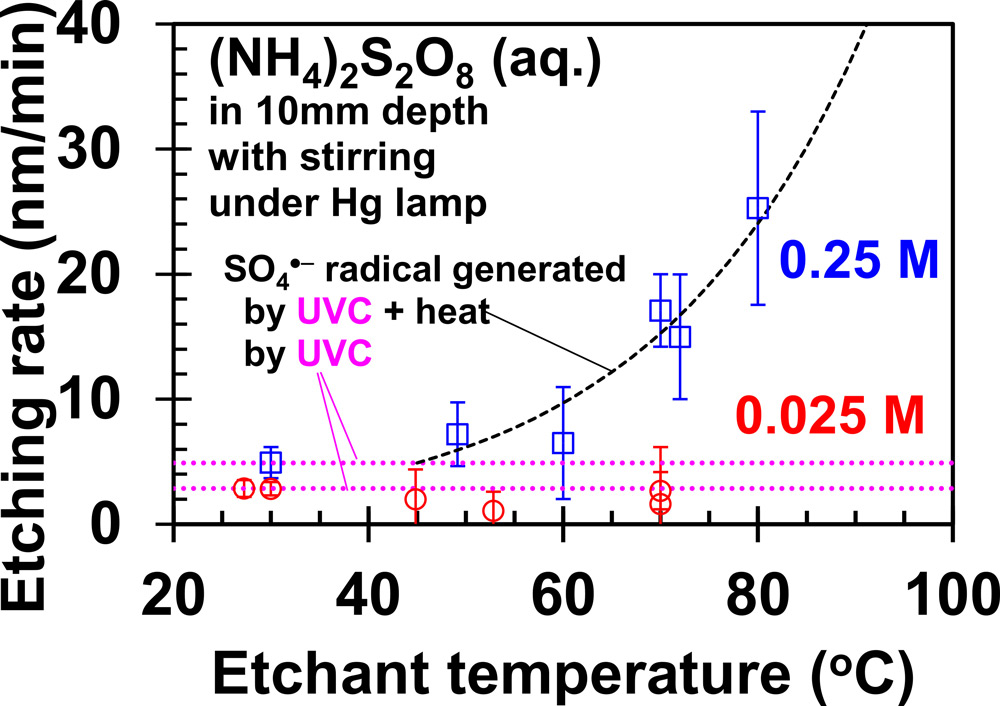
Figure 1: Etch rate versus electrolyte temperature. Broken lines: eye guides of trends for SO4·− radicals produced from S2O82- ions by heat or UVC.
The heating and high (NH4)2S2O8 concentration enabled higher etch rates of around 25nm/minute at 80°C, compared with around 5nm/minute at room temperature (Figure 1). The researchers claim the 25nm/minute value was “approximately 10 times higher than that reported by previous studies because of the high generation rate of SO4·−.” The low 0.025M-concentration electrolyte did not show a noticeable thermal effect.
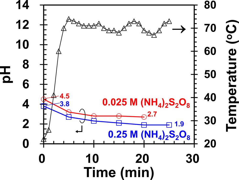
Figure 2: Temperature and pH against process time in thermal-assisted CL-PEC etch experiment.
The change seems to be related to the greater acidity of the 0.25M solution at high temperature, as indicated by lower pH (Figure 2). The applied heat split more of the S2O82- into sulfate radical SO4·− anions. The etch process in terms of redox electron and hole transfers is given as:
GaN + photocarriers (3h+ + 3e-) + 3SO4·−
→ Ga3+ + 3SO42- + ½N2(g)↑
GaN Contactless photo-electrochemical etch Wet etch MOVPE
https://doi.org/10.35848/1882-0786/ab7e09
The author Mike Cooke is a freelance technology journalist who has worked in the semiconductor and advanced technology sectors since 1997.


