


News: Optoelectronics
21 May 2020
University of Tokyo makes record-mobility tin oxide thin films with transparent properties
Researchers at the University of Tokyo have achieved the highest mobility among thin films of tin dioxide ever reported (Michitaka Fukumoto et al, ‘High mobility approaching the intrinsic limit in Ta-doped SnO2 films epitaxially grown on TiO2 (001) substrates’, Scientific Reports 10, article no. 6844). This high mobility could allow the creation of thin and even transparent tin dioxide semiconductors for use in next-generation LED lights, photovoltaic solar panels or touch-sensitive display technologies, it is reckoned.
When tin and oxygen are combined in a certain way to become tin dioxide (SnO2), the material can be made into a wide-bandgap oxide semiconductor. Because of its high mobility, since the 1960s tin dioxide has found effective use in industrial applications like gas sensors and transparent electrodes for solar devices, as well as field-effect transistors. However, the high mobility of tin oxide only existed in large bulk crystals, until now.
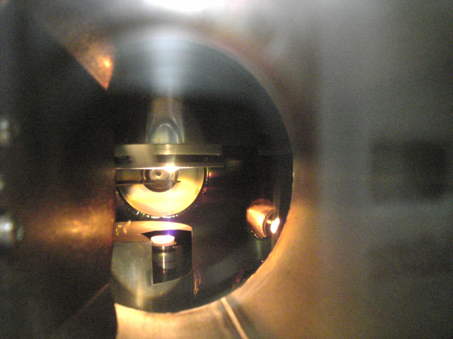
Picture: Laser deposition: a focused laser is used to create thin films of tin dioxide. © 2020 Nakao et al.
Nakao and his team made lightly tantalum (Ta)-doped SnO2 (Sn1−xTaxO2, TTO) thin films epitaxially grown on titanium dioxide TiO2 (001) substrates by pulsed laser deposition (PLD) and investigated the transport properties. The carrier density (ne) of the TTO films was systematically controlled by x. Optimized TTO (x = 3x10⁻³) films with ne ~ 1020cm−3 exhibited a very high Hall mobility (μH) of 130cm2V−1s−1 at room temperature.
“We demonstrated the highest mobility in a thin film of tin oxide ever achieved,” says Shoichiro Nakao, a researcher in the University of Tokyo’s Department of Chemistry.
The μH value coincided well with the intrinsic limit of μH calculated on the assumption that only phonon and ionized impurities contribute to the carrier scattering. The suppressed grain-boundary scattering might be explained by the reduced density of the {101} crystallographic shear planes.
“Our method of production was key to creating a substance with these properties. We used a highly focused laser to evaporate pellets of pure tin dioxide and deposit or grow material exactly how we wanted it,” says Nakao. “Such a process allows us to explore different growth conditions as well as how to incorporate additional substances. This means we can endow tin dioxide semiconductors with high mobility and useful functionality,” he adds.
“Improved mobility not only enhances the conductivity but also the transparency of the material,” notes Nakao. “Generally, transparency and conductivity cannot coexist in a material. Typical transparent materials such as glass or plastic are insulating, whereas conducting materials like metals are opaque. Few materials exhibit transparent conductivity.”
The tin oxide thin film allows visible light and near-infrared light to pass. This is a great benefit to the power conversion efficiency of photovoltaic solar panels, but other uses could include enhanced touch-screen displays with even better accuracy and responsiveness, or more efficient LED lights, it is reckoned.


