


News: Optoelectronics
15 May 2020
Seeking lower-cost non- and semi-polar gallium nitride light-emitters
University of California Santa Barbara in the USA has been developing techniques to grow and separate gallium nitride (GaN) semi-polar and non-polar epitaxial layer overgrowth (ELO) bars on native substrates [Srinivas Gandrothula et al, Appl. Phys. Express, vol13, p041003, 2020]. Such material could lead to lower-cost manufacturing of efficient light-emitting diodes (LEDs) and laser diodes, particularly for longer green and beyond wavelengths greater than 500nm.
The hope is that the process would lead to recycling of the prohibitively expensive GaN native growth substrates. The non-/semi-polar crystal orientation can eliminate or even reverse spontaneous or strain-dependent electric fields in devices, which inhibit the recombination of electrons and holes into photons in the usual polar c-plane GaN and associated heterostructures. The researchers see potential for automotive headlights, specialty lighting, displays, augmented reality/virtual reality (AR/VR) and light fidelity communication.
Although the researchers have not produced functional devices on the bars, they comment: “We believe that the demonstrated top width of ELO bars on several semi-polar planes can comfortably accommodate micro-LEDs or edge-emitting lasers, including electrical pads.” Also, last year, the UCSB group used a related technique to produce laser bars with a low threshold current density of 2.15kA/cm2 [Takeshi Kamikawa et al, Optics Express, vol27, p24717, 2019].
The process began with deposition of 200nm silicon dioxide (SiO2) on the non- or semi-polar bulk GaN. The SiO2 was patterned with 20μmx1.2mm rectangular stripes in an array of period 80μm and 1.3mm in the two dimensions, respectively (Figure 1). The stripes were oriented perpendicular to the a-direction of the GaN crystal structure. The SiO2 was etched with buffered hydrochloric acid down to the GaN substrate.

Figure 1: (a) ELO mask design on native semi-polar GaN substrate, (b) schematic of grown ELO bars from open window, (c) magnified top-view scanning electron microscope mages of ELO bars, (d) left and right vertical axis, respectively, indicate top width and vertical to horizontal growth of semi-polar ELO bars against angle measured from m-plane.
The opened stripes were used as seeds for metal-organic chemical vapor deposition (MOCVD) of GaN, creating uncoalesced ELO bars. The GaN growth conditions were 1210°C, 100Torr, using ammonia and trimethyl-gallium precursors in hydrogen carrier gas. The growth resulted in ~10μm thick bars after 4 hours.
The separation process began with removal of the SiO2 mask by hydrofluric acid. Dicing tape was placed on the GaN ELO bars, before plunging the material into liquid nitrogen at 77K cryogenic temperatures for a minute or two. The GaN was returned to room temperature by blowing nitrogen gas on the structure. As the researchers slowly pealed the dicing tape from the GaN, the ELO bars separated from the main substrate. The separation did not occur without cryogenic treatment.
The researchers explain: “Our understanding is that, by rapidly reducing the temperature, cracks were induced at the weakest portion of the ELO bars, the interface between the open window of substrate and the MOCVD grown epitaxial layer, and that the cracks propagated along the easily cleavable m-plane lying near the substrate surface to separate the ELO bars.”
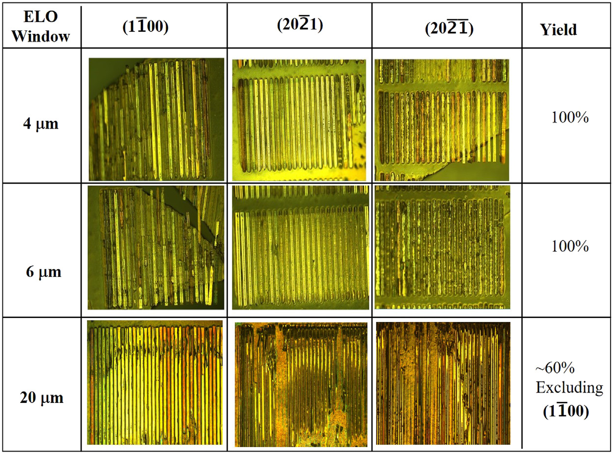
Figure 2: Removed GaN ELO bars of (1-100), (20-21) and (20-2-1) on dicing tape.
Reducing the stripe width below 10μm resulted in a few broken bars being lifted away with the tape, but almost 100% yields (Figure 2). For 20μm wide window, the bar yield was around 60%. For semi-polar ELO bars, the surface presented a series of steps with non-polar m-plane facets.
Meanwhile, the growth substrate showed some cratering in the region where the bars were separated, up to around 3μm. The researchers hope in future to control this growth substrate damage, enabling reuse.
Semi-polar GaN light-emitters GaN ELO MOCVD
https://doi.org/10.35848/1882-0786/ab7bc9
https://doi.org/10.1364/OE.27.024717
The author Mike Cooke is a freelance technology journalist who has worked in the semiconductor and advanced technology sectors since 1997.


