


News: Optoelectronics
21 May 2020
Phosphorus-free S-band indium arsenide quantum dot lasers on SOI
Researchers based in China claim the first 1.5μm-wavelength indium arsenide (InAs) quantum dot (QD) laser on silicon-on-insulator (SOI) substrate without phosphorus-based intermediate layers [Wen-Qi Wei et al, Optics Letters, vol45, p2042, 2020].
The team from Wuhan University, Beijing National Laboratory for Condensed Matter Physics and Institute of Physics, and Songshan Lake Materials Laboratory, hope for deployment in photonic integrated circuits (PICs) on silicon. The 1.5μm infrared wavelength falls in one of the major optical communications bands – for S-band optical fibers, covering 1460nm-1530nm. The team sees their work as potentially providing “a cost-effective and compact platform to realize the on-chip light source of PICs for long-haul telecommunications”.
The SOI layers were produced in a dual-chamber III-V/IV semiconductor solid-source molecular beam epitaxy (MBE) system: 3μm buried silicon dioxide (BOX), and 340nm silicon top layer. The substrate was then patterned and dry etched with 280nm deep U-shaped trenches with 360nm period and 220nm spacing. The trenches were oriented along the [110] direction of the silicon crystal lattice.
The researchers then grew further silicon and gallium arsenide (GaAs) layers over the trenches, which left hollow gaps with (111) facets in the region of the trenches (Figure 1). The technique was based on previous work that was shown to result in ultralow-defect-density material.
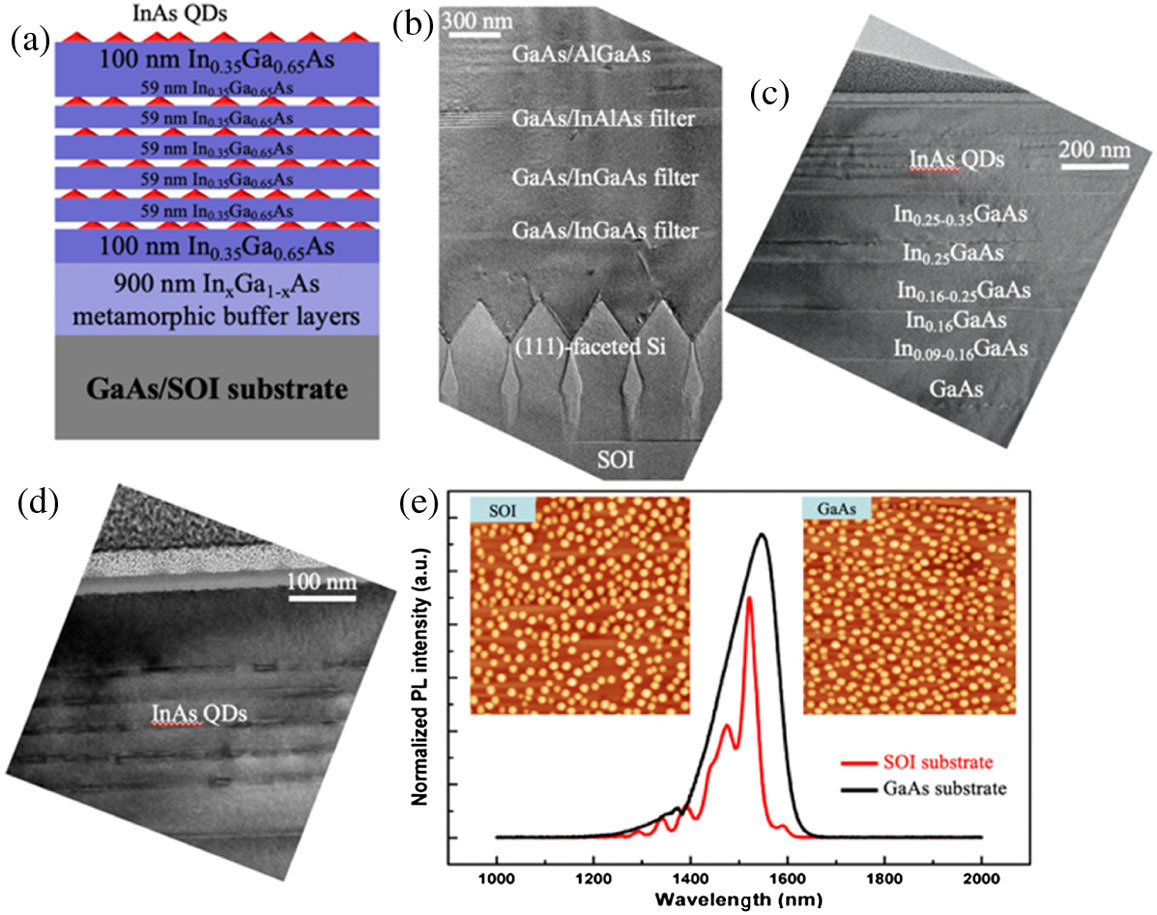
Figure 1: (a) Schematic diagram of five-layer QDs grown on GaAs/SOI platform with InGaAs metamorphic buffer layer. (b)–(d) Cross-sectional transmission electron microscope images of GaAs-on-SOI template, InAs/InGaAs metamorphic structure, and InAs QDs, respectively. (e) Room-temperature PL spectra of five-layer QD structure on SOI (red curve) and GaAs (black curve) substrates. Inset: 1μmx1μm atomic force microscope images of surface QDs.
Further epitaxial layers included a dislocation filter with InGaAs/GaAs and indium aluminium arsenide (InAlAs)/GaAs quantum well structures designed to block threading dislocations from reaching the active photonic region. A further GaAs/AlGaAs superlattice was aimed at giving a smooth surface for subsequent growth.
In between the filter layers/superlattice the indium content of the InGaAs buffer material was increased in steps from 9% to 35%. The growth temperature was relatively low, at 380°C. Thermal cycle annealing at 510°C was carried out to further smooth the layer surfaces.
The QD layers consisted of 3.1 monolayer InAs, followed by In0.35Ga0.65As layers: a 14nm 425°C cap and a 45nm 500°C spacer.
Photoluminescence (PL) spectra showed that material with five layers of QDs on SOI produced a peak that was 80% that of a similar structure grown on pure GaAs substrate. The corresponding dot densities were 3.56x10¹⁰/cm2 and 4.24x10¹⁰/cm2, according to atomic force microscopy. The PL spectra on SOI had multiple peaks, which the team suggests could be due to varying Fabry-Perot cavity interference effectjs from reflections at the underlying grating in the hollow SOI and the top surface of the sample.
Samples with seven QD layers were processed for microdisk fabrication. The epitaxial material also included 600nm In0.35Ga0.13Al0.52As as a sacrificial layer for the etch process used in fabrication. This layer was also used to create a supporting pillar for the microdisk (Figure 2). InGaAlAs layers were also used as 30nm cladding layers around the QD active region.
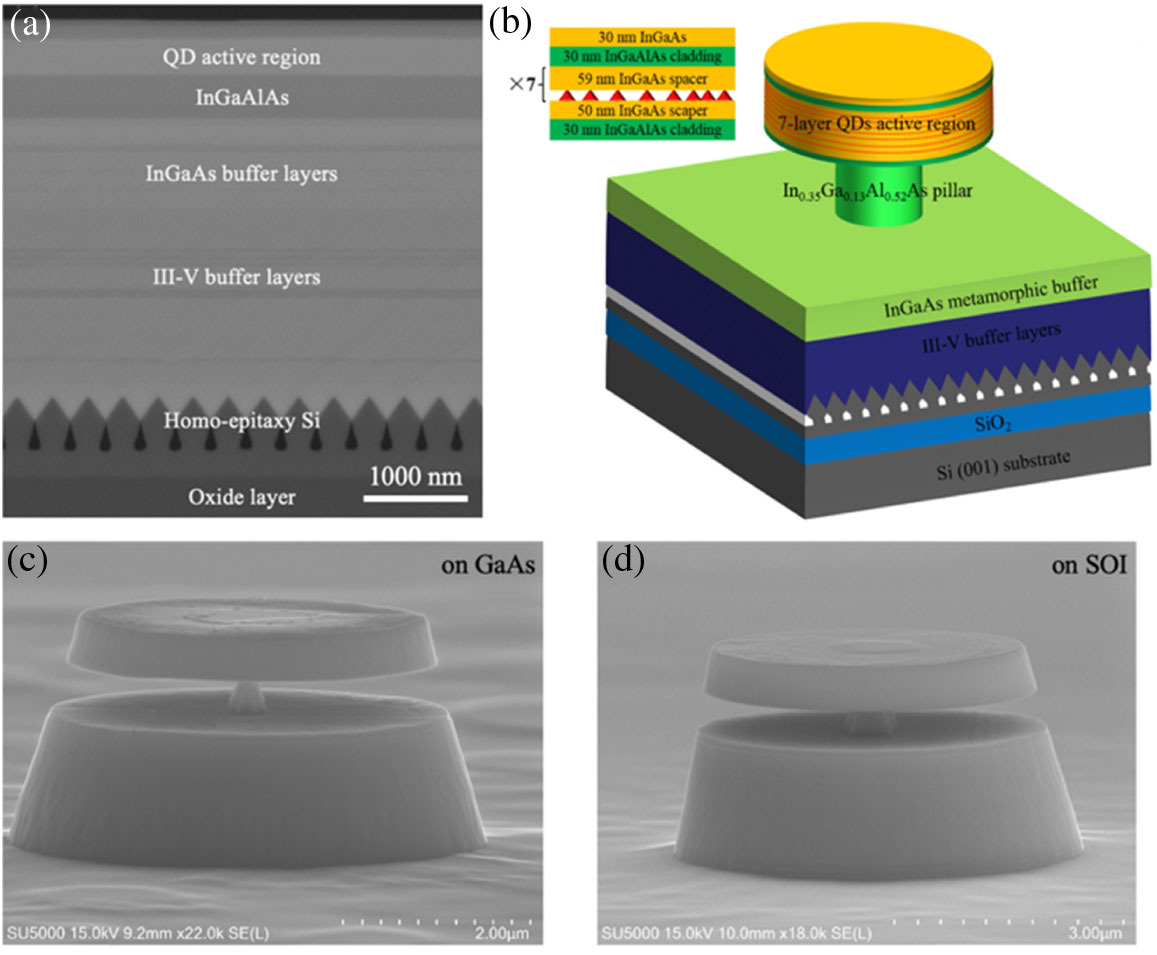
Figure 2: (a) Cross-sectional scanning electron microscope (SEM) image of microdisk sample on SOI substrate. (b) Schematic of microdisk laser. Inset: schematic of active region. (c), (d) Tilted SEM images of microdisk lasers on GaAs and SOI platforms.
The microdisks were fabricated by using silica beads as hard masks for a two-step etch process: mesa etching, using a dry plasma process, followed by a dip in hydrochloric acid, under-cutting the disks, removing InGaAlAs material and creating the support pillars.
The lasing experiments were carried out on 4μm-diameter microdisks at 200K. The optical pumping power for threshold was found to be 234μW for devices on SOI substrate, compared with 43μW for microdisks on pure GaAs substrates. The researchers suggest that the much increased threshold on SOI was due to lower optical gain of the QDs and a lower rate of heat dissipation in the silicon dioxide layer relative to GaAs.
The laser spectrum consisted of two main peaks at 1468nm and 1428nm on GaAs, and at 1512nm and 1467nm on SOI. The SOI microdisk spectra also experienced some red shift as the pump power increased, further indicating thermal effects.
Along with improving the thermal management for room-temperature operation, the team hopes to reduce the buffer thickness to enable laser-waveguide coupling for PIC applications. The researchers write: “To solve this issue, we intend to grow an embedded III–V laser structure on the bottom silicon of the SOI substrate (beneath the BOX layer) to allow butt coupling, by pre-patterning the laser epi-area on the SOI substrate.”
InAs quantum dot lasers InAs GaAs MBE SOI PICs
https://doi.org/10.1364/OL.389191
The author Mike Cooke is a freelance technology journalist who has worked in the semiconductor and advanced technology sectors since 1997.


