


News: Suppliers
26 October 2020
IGaN achieves low conduction loss with 150mm GaN-on-Si epi for RF applications
In recent years, there has been growing demand for GaN-based products stemming from the increased adoption of GaN power and RF devices in a variety of applications, notes Singapore-based IGSS GaN Pte Ltd (IGaN) – which develops and commercializes gallium nitride-on-silicon/silicon carbide (GaN-on-Si/SiC) epitaxial wafers and proprietary 8” (200mm) GaN fabrication technologies for power, RF and sensor applications. From military, defence, aerospace and next-generation telecommunications (particularly with 5G networks), the wide bandgap of GaN-based materials offers remarkable breakdown electric field and high drift velocity suitable for the fabrication of high-power and high-frequency devices.
In terms of applications, III-nitride materials such as GaN are generally grown heteroepitaxially on a substrate. Among various substrate materials, silicon is widely selected for the growth of an epitaxial stack comprising III-nitride materials due to the lower substrate cost and flexible scalability on substrate size. Differences in material properties such as thermal expansion coefficient and lattice constant between III-nitride materials and the silicon substrate can pose technolical challenges (i.e. cracks, defects, wafer bow and crystal quality) for practical applications. However, despite the great promise shown by GaN-on-Si RF electronics, there remain a few issues to be resolved.
One such issue is the presence of a parasitic channel formed at the III-nitride/silicon interface, which leads to parasitic loss, severely degrading the output power, power gain and efficiency of devices especially when they are operating at high frequency. A key requirement in GaN high-electron-mobility transistors (HEMTs) on silicon for RF applications is the reduction in conduction loss at the AlN/Si interface. As the AlN/Si interface can become conductive due to the doping of Al and Ga residuals in the reactor, preconditioning of the reactor and the growth conditions of the first AlN layers on the silicon substrate will be crucial for the suppression of conduction loss.
IGaN claims that its technology has the unique advantage of achieving very low conduction loss, meeting the industry standards for GaN HEMTs on silicon for RF applications. Recently processed IGaN 150mm GaN-on-Si HEMT wafers have achieved a conduction loss of 0.15dB at room temperature and 0.23dB at high temperature for an operating frequency of 10GHz. The Figure shows measurements of conduction loss up to an operating frequency of 10GHz at room temperature and high temperature. Low conduction loss is a key factor for achieving low RF loss, which is critical for RF devices.
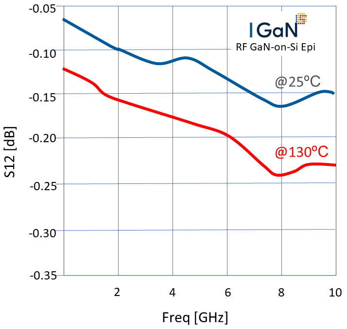
Figure: Conduction loss measurement at room temperature and high temperature up to an operating frequency of 10GHz on IGaN GaN-on-Si HEMT wafer.
Besides the conduction loss test, IGaN has implemented a quick method for screening-out poor-performing GaN epiwafers before fab processing that can save customers expensive scrappage and help to avert potential wastage of processed wafers and packaged devices downstream if the epiwafer substrates has high conduction losses. Early detection of high-conduction-loss epiwafers is critical for the mass production of RF GaN devices, says IGaN.
RF Epistack on 200m substrates is under development and will be available to customers by the end of first-quarter 2021.
IGaN establishing $73m GaN Epi Centre by mid-2021
IGaN launches MPW shuttle program for GaN-on-Si transistors


