


News: Optoelectronics
22 October 2020
AlPN vapor phase epitaxy on GaN
Nagoya University and National Institute for Materials Science (NIMS) in Japan report on aluminium phosphide nitride (AlPN) vapor phase epitaxy (VPE) on gallium nitride (GaN) that results in low 150Ω/square sheet resistance material [Markus Pristovsek et al, Appl. Phys. Express, vol13, p111001, 2020].
The low resistance promises power electronics applications such as high-electron mobility transistors (HEMTs). Another potential arises from an increased refractive index contrast relative to III-nitride alternatives for distributed Bragg reflectors (DBRs) in short-wavelength vertical-cavity surface-emitting lasers (VCSELs).
The alloying of P and N to give AlGaPN semiconductor material has previously been proposed in patent form (now expired). The Nagoya/NIMS researchers express scepticism as to whether the process described in the patent was ever realized, since there was no subsequent supporting publication.
GaPN alloys have been studied to an extent, but suffer from problems such as P substitution on the Ga-site, rather than the desired N-site, even forming P3N3 domains. This relates to the covalent radius of P (107pm) being closer to that of Al (121pm) and Ga (122pm), relative to N (71pm). However, the tensile strain of AlN on GaN should favor P incorporation on the group-V N-site, avoiding this problem.
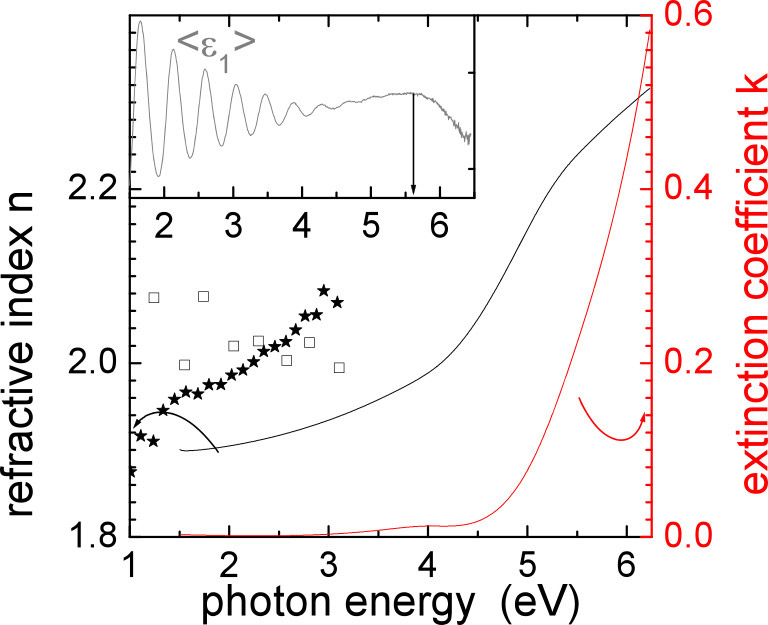
Figure 1: Refractive index and extinction coefficient averaged from three AlP0.13N0.87 layers of 180nm, 315nm and 655nm on GaN-sapphire. Points from vertical incidence reflection measurements of 315nm (open box) and 655nm (star) AlPN. Inset: effective <ε1> dielectric constant of 655nm AlPN on 22μm carbon-doped GaN on sapphire, to suppress GaN Fabry-Perot oscillations.
The source of the phosphorus component of the AlPN was tertiary-butylphosphine (tBP). This organic compound was chosen over the simpler carbon-free ammonia-analogue phosphine/phosphane (PH3), due to its lower toxicity, high vapor pressure, and low decomposition temperature. In fact, the laboratory where the material was grown is not permitted to handle PH3 due to safety considerations.
The lead author, Markus Pristovsek, comments that he began his scientific career around the year 2000 at Germany’s Technical University Berlin (TUB), looking for alternative precursors of arsenic and phosphorus for VPE, finding tBP and tBAs to give the best performance.
The AlPN was grown on c-plane (0001) GaN/sapphire templates through metal-organic VPE. The other precursors were trimethyl aluminum (TMAl) and ammonia (NH3). Hydrogen gas (H2) was used to carry the precursors to the deposition reactor chamber.
Initially the researchers switched on the tBP and TMAl together, but later found that starting with a few seconds of tBP flow improved the AlPN quality. The tBP and NH3 flow was also maintained during the initial cooling after growth at 1050-1250°C, down to 950°C.
The team used an empty metal-organic line for the tBP, but this is known to cause gas-phase reactions in AlGaP growth with TMAl/tBP pre-reactions occurring in the lines and showerhead. In future work, the researchers plan to use a group-V inlet to try to avoid these problems. One result of these drawbacks was a gradient in the P-content of grown material, leading to cracking.
The initial experiments explored the effect of tBP partial pressure on the grown material. The researchers found that an increased tBP partial pressure reduced cracking of the material.
X-ray diffraction on 7nm/14nm AlPN/GaN superlattices found an incorporation limit of 18-20%, based on the disappearance of satellite peaks. The researchers attributed the limit to compressive strain arising in the superlattice. Compressive strain has a similar effect on GaPN growth. At the pure AlN extreme, the strain in the superlattice is tensile.
Thicker lattice-matched AlPN layers were found to be dark, unlike AlN, which is transparent to visible light. The team suggests that carbon (C) from the tBP precursor is to blame. The high temperatures result in the presence of high numbers of single CHx radicals.
The researchers explain: “The tBP partial pressure is about 50x higher than the TMAl partial pressure, and tBP contains four carbon atoms instead of three for TMAl. Hence, during AlPN growth about 70x more CHx radicals are present than for AlN growth.”
Increasing the ammonia partial pressure was found to enable almost transparent 100nm layers of AlPN to be grown with little impact on P incorporation. The ammonia increased the supply of active hydrogen atoms, reducing the radical concentration.
The researchers aimed to grow a lattice-matched AlPN layer with 10.6% P, but x-ray diffraction revealed the P content to be fractionally lower at 10.3%, giving a slight tensile strain.
Ellipsometry measurements gave refractive indices in the range 1.95-2.05, close to the values found for pure AlN. These values give a difference relative to GaN about 2x that of Al0.83In0.17N, which could be useful for the construction of distributed Bragg reflectors in vertical-cavity surface-emitting lasers. The team reports: “A Bragg mirror from AlP0.11N0.89 could reach 99% reflectivity with only 14 pairs for wavelengths between 300 and 550nm.”
The growth rate was relatively high at 700nm/hour. Considering that the process did not need temperature ramping or gas exchanges, the researchers suggest that a Bragg mirror could be produced in less than 3 hours, in contrast to the 12 hours for AlInN mirrors, once problems like material cracking during growth are sorted.
Experiments on a 655nm layer of AlP0.13N0.87 showed Fabry-Perot oscillations up to around 5.5eV, suggesting this as being the region of the optical bandgap. Such a value would suggest a smaller bandgap bowing parameter for the AlN-AlP alloy system of 3eV, compared with 9eV for GaN-GaP. A more precise bandgap assessment using cathodoluminescence was “inconclusive”.
Resistance mapping of an unoptimized sample gave a sheet value of (150±50)Ω/square for the two-dimensional electron gas arising from the high charge polarization contrast of the AlPN and GaN material. The researchers comment: “A mean value of 150Ω/square would be an excellent value for an AlInN/AlN/GaN heterostructure, and at least on the same order as the Al1-xScxN system, which is expected to have a high polarization too.”
One possible problem with AlPN is oxidation in air. Cubic AlP is known to oxidize in seconds to Al2O3, releasing PH3. Indeed, this is one technique for creating Al2O3 surface passivation. Although the researchers found their AlP0.13N0.87 to be less susceptible to oxidation, it did dissolve within a minute in an alkaline developer. “On the positive side, this makes AlPN an easily removable, lattice-matched sacrificial layer,” the team writes.
An AlP0.13N0.87 sample from the initial growth experiments without tBP pre-flow was found to contain 10-20% oxygen after storage in air for two months, according to an energy-dispersive x-ray spectroscopy (EDS) and transmission electron microscope (TEM) study (Figure 2). At the same time, an abrupt ~5nm interface between the AlPN and GaN template was observed in the same material. With other materials, such as aluminium indium nitride (AlInN), there is often a problem with Ga incorporation.
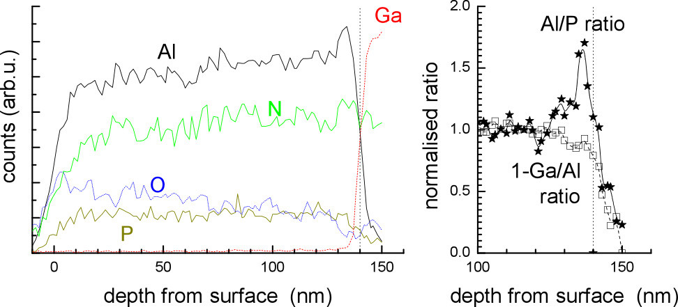
Figure 2: TEM-EDS trace from 140nm AlPN layer after storage in air for about 2 months (left). Ga signal reduced by 3x while N, P and O increased 2.5x. Vertical line marks GaN interface. Wedge shape of TEM slice gives EDS gradient towards surface. Right: normalized (1-Ga)/Al ratio (open box) and Al/P ratio (star).
However, within 30nm of the GaN the P content was lower than desired. The researchers comment: “This P-deficient layer is probably the reason why we had observed sometimes cracking even for lattice-matched layers before we introduced the tBP-preflow.”
AlPN AlGaPN VPE GaN VCSELs HEMTs
https://doi.org/10.35848/1882-0786/abbbca
The author Mike Cooke is a freelance technology journalist who has worked in the semiconductor and advanced technology sectors since 1997.


