


News: Optoelectronics
15 October 2020
InGaN laser with n-type ridge on silicon
China’s Suzhou Institute of Nano-Tech and Nano-Bionics (SINANO) has fabricated indium gallium nitride (InGaN) violet-emitting laser diodes (LDs) on silicon with n-type ridge waveguides (nRWs), which demonstrated lower electrical resistance and improved thermal performance over pRW-LDs [Rui Zhou et al, ACS Photonics, published online 23 September 2020]. Normally, process limitations dictate that the RW in InGaN-based laser diodes are on the p-side of the device. The thermal and electrical problems arise because p-GaN is much more resistive than n-GaN.
The team, which also included a researcher from Tsinghua University in China, believes that nRW-LD devices could be fully compatible with large-scale silicon-based complementary metal-oxide-semiconductor (CMOS) mainstream electronics and could be used in monolithically integrated silicon photonics as an efficient on-chip light source for high-speed data communication and computation.
Magnesium (Mg) is the usual p-type dopant in III-nitride structures. This imposes a number of restrictions in the growth and activation annealing required to create p-type conductivity. First, Mg tends to hang around in reaction chambers. This ‘memory effect’ means that subsequent layers will have some level of Mg incorporation, whether desired or not. The memory effect therefore tends to result in growth processes being designed with p-type layers being grown last.
Also, Mg-doped GaN/InGaN is passivated (i.e. rendered ineffective) with hydrogen incorporation. A key part of activation of the p-type layers consists in driving out this hydrogen, usually by raising the temperature in an annealing process, encouraging diffusion of these atoms out of the structure. This requires the hydrogen to travel as small a distance as possible before exiting the material.
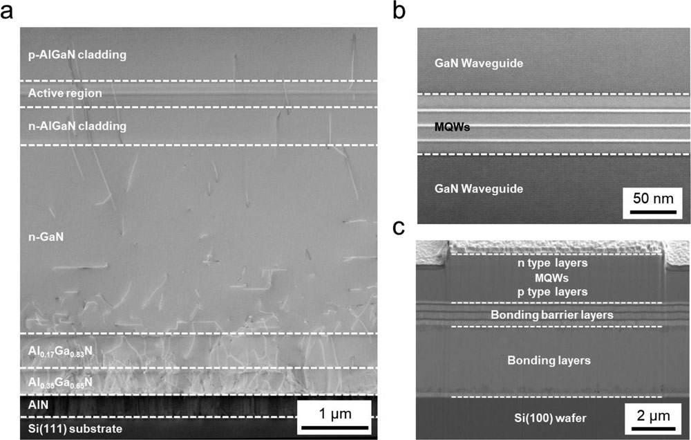
Figure 1: Cross-sectional images of nRW-LD structures. (a) Scanning transmission electron micrography of nRW-LD epitaxial structure on Si(111) substrate. (b) Enlarged image of InGaN/GaN quantum wells. (c) Cross-sectional scanning electron micrograph of device bonded to Si(100) wafer.
The III-nitride heterostructure for the RW-LDs was grown on silicon with (111) crystal orientation. Measures were taken to control threading dislocation density. The laser diode structure consisted of five InGaN quantum wells sandwiched between waveguide layers (Figure 1). The n-side waveguide and the nearest 50nm of the cladding were undoped, avoiding current spreading in the ridge-waveguide structure.
The laser diode structure was bonded p-side down to an exact Si(100) wafer with a p-type ohmic contact electrode surface. The Si(111) growth substrate was removed with wet etching. Further dry plasma etch removed the AlN/AlGaN growth buffer structures. The inverted RW-LD structure allows the n-type side of the cladding to be much thinner than usual, ~0.5μm. In non-inverted structures the n-cladding lies on top on a thick GaN template, which has an ‘anti-guiding’ effect. The p-side of the inverted RW-LD cladding was thicker, at 1.2μm.
The researchers comment: “The thickness reduction of the n-type AlGaN cladding layer with a low thermal conductivity can largely decrease both the thermal resistance and the tensile stress resulting from the lattice mismatch between AlGaN and GaN template, which boost the device performance and fabrication yield.”
The bonded material was finally fabricated into 10μmx800μm RW-LD devices (Figure 2). The effective area of the p-electrode was estimated to be 300μmx800μm.
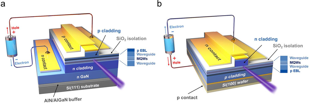
Figure 2: Schematic architecture of InGaN-based (a) pRW-LD on Si(111) and (b) nRW-LD on Si(100).
The reverse leakage current was ~10-7A at -5V reverse bias. The turn-on voltage was around 3.0V. Increase in bias beyond this gave much higher current injection in the inverted RW-LD, compared with a normal pRW-LD on Si(111). This reflected the lower series resistance on the wider p-type region.
The differential resistance at 350mA injection into the inverted nRW-LD was 1.2Ω, compared with 2.3Ω for the normal pRW device. This reduced the operation voltage 1.41V to 4.15V. The lower voltage meant reduced Joule heating, delaying thermal degradation of laser performance. The inverted device thermal resistance was estimated to be 18.2K/W, compared with 26.5K/W for the normal p-ridge laser diode. The junction temperatures under continuous wave (CW) operation at 350mA were 48.5°C and 73.5°C, respectively. The 25°C lower junction temperature was attributed to the lower Joule heating and to the shorter heat dissipation path length.
There is also scope for improvement, since the researchers used nickel-tin solder in the wafer bonding process, which has a relatively low thermal conductivity. A copper-based alternative could be a way forward to an even better thermal performance.
The nRW-LD structure had a 12nm full-width at half maximum (FWHM) spectral line at 100mA injection (Figure 3). The linewidth narrowed to 0.8nm at 320mA, giving a laser mode wavelength of 418.3nm at threshold.
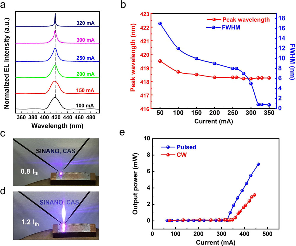
Figure 3: Electroluminescence of nRW-LD under electrical injection. (a) Spectra under pulsed currents (0.4% duty cycle, 10kHz repetition rate) at room temperature (RT). (b) Peak wavelength and FWHM of spectra versus pulsed injection current at RT. (c, d) Far-field patterns observed 0.8x and 1.2x threshold current. (e) Light output power versus pulsed and CW injection current at RT.
The threshold current density of 4.37kA/cm2 is seen as high relative to state-of-the-art InGaN laser diodes under CW operation. The lifetime was also only 5 minutes before “a drastic degradation of output power” was observed. The researchers blame a high 6x10⁸/cm2 threading dislocation density and an unoptimized active region. Threading dislocations provide non-radiative recombination centers and leakage current paths that sap efficiency and reliability. Some studies suggest lifetimes of laser diodes can be increased to 10,000 hours by reducing threading dislocations to 106/cm2.
InGaN violet-emitting laser diodes InGaN GaN CMOS
https://dx.doi.org/10.1021/acsphotonics.0c01061
The author Mike Cooke is a freelance technology journalist who has worked in the semiconductor and advanced technology sectors since 1997.


