


News: Optoelectronics
8 October 2020
Displaced misfits boost QD laser on silicon
Researchers, mainly with University of California Santa Barbara (UCSB) in the USA, have improved indium arsenide quantum dot laser diode (InAs QD LD) performance on silicon (Si) by introducing layers designed to shift misfit dislocations (MDs) away from the dot-in-well (DWELL) active light-generating region [Jennifer Selvidge et al, Appl. Phys. Lett., vol117, p122101, 2020].
The team, which included researchers from Korea Institute of Science and Technology (KIST) and Intel Corp in the USA, comments: “Our results suggest that devices employing both traditional threading dislocation reduction techniques and optimized misfit dislocation trapping layers may finally lead to fully integrated, commercially viable silicon-based photonic integrated circuits.”
Such technologies are hoped to increase data network bandwidth and energy efficiency, along with other applications in chip-scale sensing, detection, and ranging. Direct growth of III-V optoelectronic semiconductors on silicon should reduce production costs through economies of scale.
Up to now, devices have suffered from performance challenges that have often been blamed on high threading dislocation densities (TDDs), which create non-radiative recombination centers. However, the UCSB/KIST/Intel team has recently found that misfit dislocations can also sap quantum DWELL efficiency.
The team explains: “These <110>-oriented misfit dislocations, like threading dislocations, limit performance and reliability because they, too, are potent non-radiative recombination centers. Worse still, they may be far more damaging as they have a much larger interaction area with the active region.”
The researchers suggest that the low number of reports of misfit dislocations in III-V heterostructures is due to the difficulty in seeing them in cross-sectional transmission electron microscopy (TEM) with QD strain contrast masking that from misfit dislocations.
The researchers believe that the misfit dislocations form during cool-down from the 540°C growth temperature, not during growth, since the DWELL layer is below the critical thickness for misfit dislocation formation. The difference between the thermal expansion of gallium arsenide (GaAs) and silicon is around 3x10⁻⁶/K.
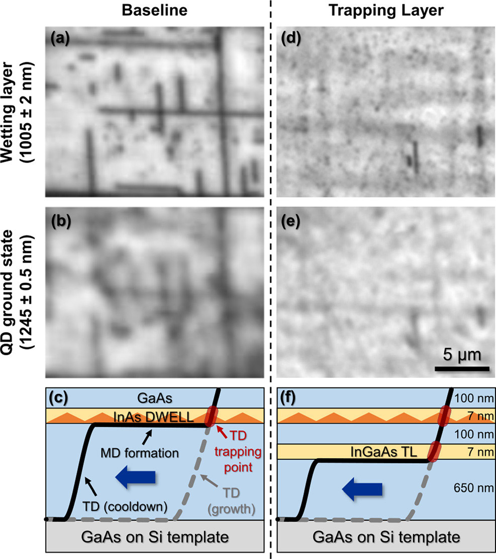
Figure 1: (a) and (b) Monochromatic cathodoluminescence (CL) images of baseline structure at (a) QD wetting-layer emission wavelength (1005nm) and (b) QD ground-state emission wavelength (1245nm). (c) Schematic of proposed dislocation evolution in baseline structure. (d) and (e) Comparable wetting/QD layer CL images for trapping layer structure (f).
At around 300°C during the cooling process, the biaxial tensile strain is about 0.1%, inducing mobile threading dislocation segments to glide in GaAs layers thicker than a few hundred nanometers, it is believed. This is not a problem in itself, but the threading dislocations passing through the DWELL layer are not so compliant, resulting in misfit dislocations close to the DWELL, creating non-radiative recombination potential (Figure 1).
The researchers comment: “We hypothesize that this mechanical hardening arises from uneven stress fields generated by the strained QDs and alloy fluctuations in the In0.15Ga0.85As QW. The latter effect, similar to alloy hardening phenomena reported previously in bulk semiconductors, occurs because the difference in covalent radii of indium (142pm) and gallium (124pm) generates in-layer stress fluctuations.”
No misfit dislocation structures were seen above the DWELL since the GaAs cap layer was too thin for threading dislocation gliding. In fact, the team saw placing a thin glide-free layer between the misfit dislocation and the DWELL as a means to improve performance. This was achieved by inserting a 7nm In0.15Ga0.85As trapping layer (TL) about 100nm below the DWELL.
The researchers then produced laser structures, fabricated into 3μmx1.5mm ridge-waveguide laser diodes (Figure 2). The substrate was a GaAs/Si template with 7x10⁷/cm2 threading dislocation density buffer. Since the top p-GaAs contact layer was thick enough for threading dislocation gliding to occur, the researchers inserted trapping layers 80nm above and below the five layers of DWELLs used as active layer.
![Figure 2: a) Schematic of laser with trapping layers (TLs) (red boxes) above and below QD layers. (b) Cross-sectional bright-field STEM ([100] zone) of TL laser. Inset foil orientation relative to misfit dislocations. Arrows mark misfit dislocation segments at trapping layers. (c) High-magnification image of (b).](20101_ucsb_f2.jpg)
Figure 2: a) Schematic of laser with trapping layers (TLs) (red boxes) above and below QD layers. (b) Cross-sectional bright-field STEM ([100] zone) of TL laser. Inset foil orientation relative to misfit dislocations. Arrows mark misfit dislocation segments at trapping layers. (c) High-magnification image of (b).
The indium contents of the two trapping layers were the same, but gallium was replaced with aluminium (Al) in the bottom trapping layer. The covalent single-bond radius for Al is 126pm, compared with 124pm for Ga. A ‘baseline’ device was also produced without trapping layers.
Deeper inspection using tomography techniques suggest that, even with the trapping layers, there was some threading dislocation glide, but not as extensive as without the layers. The team reports that trapping layers displace most of the misfit dislocation length from the QDs, on the basis of plan-view scanning transmission electron microscopy (STEM).
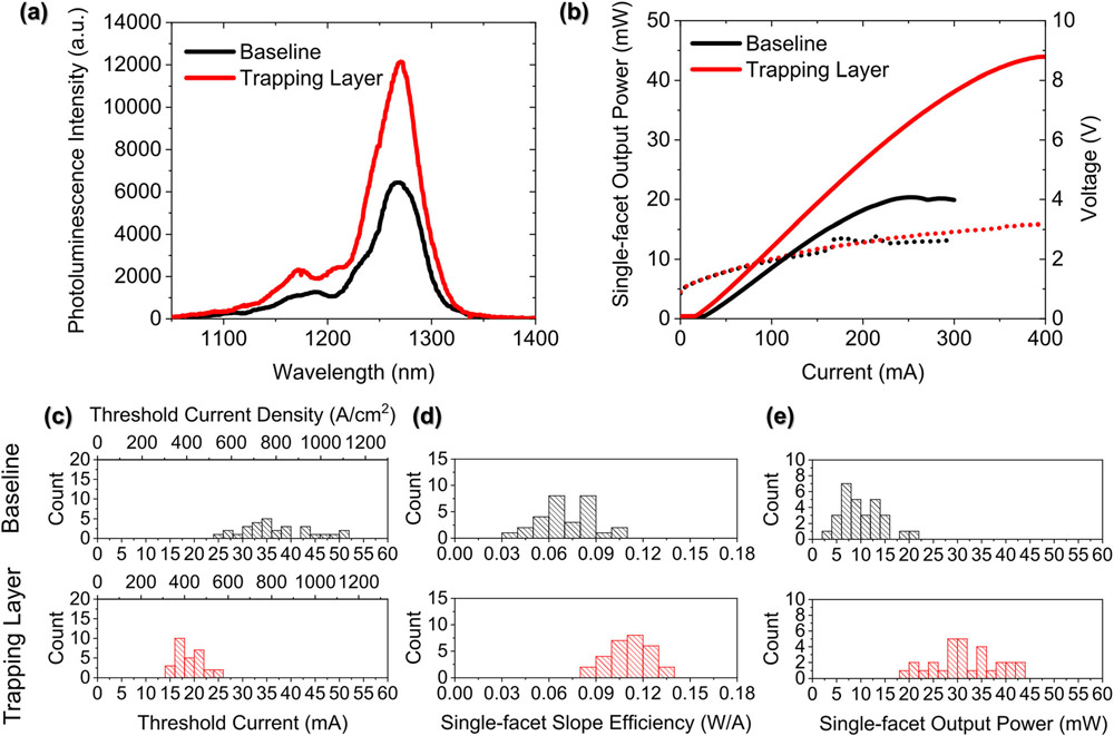
Figure 3: (a)–(e) Comparisons of baseline (black) and trapping layer (red) lasers. (a) Photoluminescence intensity. (b) Single-facet output power (solid) and voltage (dashed) as function of current. (c)–(e) Histograms showing performance improvements of trapping layer devices: (c) threshold current, (d) slope efficiency, and (e) output power.
The presence of trapping layers increased photoluminescence by almost a factor of two (Figure 3). Under electrical bias, the threshold current with trapping layers was also reduced by a factor of about two. The lowest thresholds achieved with trapping layers was 16mA, a 40% decrease on the lowest baseline value. Despite having 4x the threading dislocation density of ‘state-of-the-art’ devices on silicon reported in 2019, the threshold current with trapping layers was 20% lower in this case too.
Other improvements were shown in median slope efficiency (+60%) and median peak single-facet output power (3.4x) over the baseline laser diodes. The median input power was 0.85W before thermal roll-over with trapping layers, compared with 0.46W for the baseline. The researchers comment: “This indicates — assuming comparable thermal impedances — that the inclusion of trapping layers increases the lasers’ optical amplification (gain).”
The team sees the performance gains from trapping layers as being comparable to those achieved by reducing threading dislocation densities from 7x10⁷/cm2 to 7x10⁶/cm2.
The researchers write: “As device thicknesses are critical for many applications, it is highly advantageous that these performance gains made using thin misfit trapping layers compare favorably to those achieved using hundreds of nanometers of traditional threading dislocation filters.”
The team also suspects that reported lifetime improvements with reduced threading dislocation density could be likely explained by an “unseen reduction in the total misfit dislocation line length”, adding: “All dislocation line length, whether misfit dislocation or threading dislocation, within the active region degrades laser performance and lifetime; the inclusion and optimization of trapping layers thus complement important, ongoing threading dislocation density reduction efforts.”
Indium arsenide quantum dot laser diode InAs GaAs Misfit dislocations Dot-in-well
https://doi.org/10.1063/5.0023378
The author Mike Cooke is a freelance technology journalist who has worked in the semiconductor and advanced technology sectors since 1997.


