


News: LEDs
15 September 2020
Aledia benefits from strong patent portfolio in GaN-on-Si nanowire LEDs
Aledia S.A. was spun off from Grenoble-based micro/nanotechnology R&D center CEA-Leti in 2011 to develop a disruptive 3D LED technology based on the standard 200mm silicon platform, which would shrink the cost per chip in comparison with the conventional 2D LED technology.
Now, to address a market estimated to be worth about $120m related to displays for computers, tablets, smartphones and augmented reality (AR) glasses, earlier this year the startup announced plans to build a first manufacturing facility in the Grenoble area. Aledia plans to enter mass production of micro-displays by 2022.
Jointly with Cea-Leti, Aledia has developed the fabrication of 3D LEDs based on GaN nanowires grown on large-area silicon substrates, leading to the filing of more than 100 patent families (single inventions filed in multiple countries) since 2012, grouping more than 440 patents and pending patent applications worldwide. “Interestingly, more than 180 patent applications have already been granted, putting the emphasis on Europe (90+ patents) and the USA (50+ patents), although a significant number of patents were also granted in Asia (China: 19, Japan: 10, South Korea: 4 and Taiwan: 4),” notes Remi Comyn PhD, technology & patent analyst Compound Semiconductors and Electronics at IP strategy consulting company Knowmade. “Importantly, 29 patent families have not got a granted member yet; mostly inventions filed in the last three years and related to display applications (21),” he adds.
As of September, Aledia owns 58 patent families focused on nanowire LEDs (Figure 1a). The startup first considered residential lighting and automotive lighting as the most promising markets for its technology, explaining the presence of companies such as Ikea and Valeo among its investors. However, it eventually decided to target display applications, which translated into more than 40 additional patent families related to displays in Aledia’s portfolio, with more than 30 patent applications filed in the last three years. In the nanowire LED patent landscape, several players such as Samsung and glō are following a similar trend. As a result, patenting activity related to nanowire-based micro-displays took off in 2016/2017 and is expected to accelerate in 2020/2021 as more players race towards micro-LED commercialization (Figure 1 bottom).
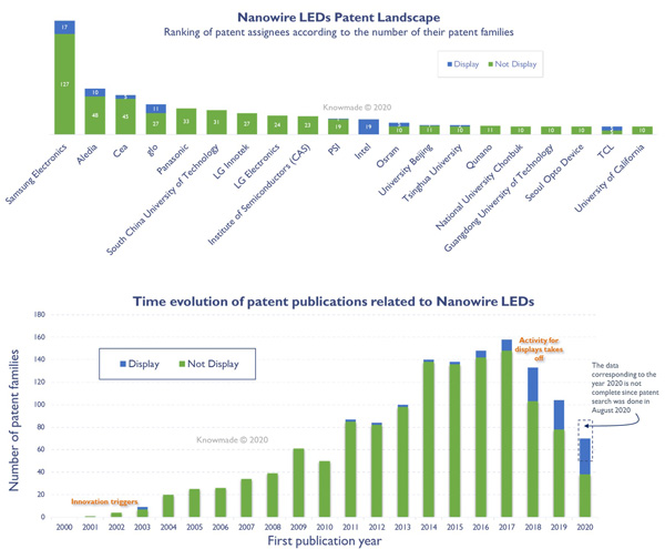
Figure 1: (top) Aledia’s main competitors in the nanowire LED patent landscape. (bottom) Timeline of publications in the Nanowire LED patent landscape.
Another component of Aledia’s strategic move towards display applications is that Intel joined the rank of investors in 2018. At the same time, the US company was identified by Knowmade as a new entrant in the nanowire LED patent landscape, with a relatively similar approach to Aledia and a strong focus on micro-LED displays (Figure 1 top). “Intel is developing manufacturing approaches for micro-LED structures and displays based on the assembly of nanowires, including GaN nanowires, on silicon substrates,” says Comyn. Indeed, Knowmade has identified 19 inventions from Intel in the nanowire LED patent landscape, mostly filed in the USA. As of September, 5 US patents have already been granted to Intel.
In 2020, Knowmade investigated the GaN-on-silicon patent landscape, in which Aledia owns 30 patent families. “Aledia’s inventions included in the GaN-on-silicon patent landscape are mainly related to the growth of the nanowire emitters in large quantities with a high degree of precision and control,” says Comyn. Additional inventions concern the fabrication of electrical contacts on GaN nanostructures (US9991342, US10340138), and device manufacturing issues (e.g. dry etching US20190172970), the removal of defective nanowires (US9299882), the monolithic integration of LEDs with devices such as transistors to control the nanowire LEDs (US10050080) or to detect the LED temperature (US20160197064). In addition, more and more display-related inventions have been identified in GaN-on-silicon lately (e.g. US10734442).
Furthermore, Aledia can rely on additional patents from its R&D partner Cea-Leti, which is well established in nanowire LEDs and GaN-on-Si for optoelectronics. The institute owns 50 patent families related to nanowire LEDs with more than 170 patents granted in the US (40+), Europe (30+), China (15) and Japan (15). Interestingly, at least five inventions focus on displays (e.g. US8890111). Also, 19 belong to the GaN-on-Si for optoelectronics patent landscape, where Cea is a well-established player (30+ inventions).
Overall, between its own patents and IP agreements with partners, Aledia benefits from a strong patent portfolio of more than 170 patent families to protect the features of its technology in view of commercialization.
In conclusion, major endeavors in R&D over the last three years to improve the nanowire LED technology for displays, together with its global IP strategy, have put Aledia in a good position to face the tough competition in an emerging micro-LED display market, reckons Knowmade.


