


News: Optoelectronics
21 September 2020
BiTeSe optoelectronic functional device
Hebei University in China has used bismuth telluride selenide (Bi2Te2.7Se0.3) to realize a range of optoelectronic functions [Hong Wang et al, IEEE Electron Device Letters, published online 17 August 2020}. The material has a two-dimensional structure with a narrow bandgap of 0.16eV. The researchers suggest that it may be possible to combine information communication, calculation and storage functions in one device in the future.
A 20nm Bi2Te2.7Se0.3 film was fabricated by pulsed laser deposition (PLD) on ~30nm native silicon dioxide (SiO2) on p-type silicon substrate (Figure 1). A 0.1mm-diameter circular palladium (Pd) electrode was added with DC magnetron sputtering. The electrode was thin enough (60nm) to allow light to pass through. The Bi2Te2.7Se0.3 film was naturally n-type with an area of 1cm2.
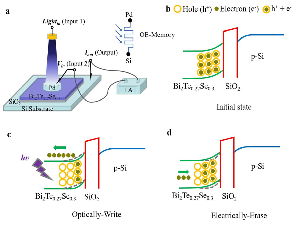
Figure 1: (a) Schematic illustration of Pd/Bi2Te2.7Se0.3/SiO2/Si device. Band diagrams of (b) initial state, (c) and under optical writing and (d) electrical erasing conditions.
The bandgaps of the Bi2Te2.7Se0.3, SiO2 and Si layers are nominally 0.16, 8.9 and 1.1eV, respectively. Optical illumination generates freely moving electron-hole pairs – the electrons move toward the Pd electrode where they are trapped, leaving a positive charge at the Bi2Te2.7Se0.3/SiO2 interface. At the same time the SiO2 barrier is lowered, even without illumination, reducing the resistance to current flow through the structure with a positive bias on the Pd electrode. The erasure of the memory state is achieved with negative bias on the Pd electrode pushing electrons back to recombine at the Bi2Te2.7Se0.3/SiO2 interface, raising the barrier and increasing electrical resistance.
The researchers used the structure to achieve ‘OR’ gate functionality with a 100mW light pulse as one input and a 2V electrical pulse as the other. The zero output state consisted of a current pulse through the structure of around 8x10⁻⁹A, while separate optical and electrical pulses gave 8x10⁻⁷A and 9x10⁻⁷A, respectively. Optical and electrical pulses combined gave 1x10⁻⁶A.
The team also looked at the potential for non-volatile resistive memory, realizing three resistance states - 298 kΩ, 4000 kΩ and 20,000kΩ - with different optical write powers (100mW, 50mW and 5mW). The data retention time was in excess of 104 seconds (just under 3 hours).
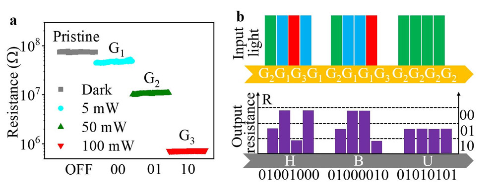
Figure 2: (a) Decoding of ‘00’, ‘01’ and ‘10’ bit pairs with light pluses at intensities of 5 (G1), 50 (G2) and 100mW (G3), respectively. (b) ‘HBU’ demodulation in eight-bit ASCII. The ‘HBU’ data did not need a code for ‘11’.
The researchers also report the use of the structure to demodulate an optical input into an electrical signal. The team successfully decoded a three-letter ASCII data stream – ‘HBU’ standing for ‘Hebei University’ - encoded on a purple light beam (Figure 2). Three resistance levels were used to encode bit pairs, giving four signals per letter, or twelve signals in total.
https://doi.org/10.1109/LED.2020.3017166
The author Mike Cooke is a freelance technology journalist who has worked in the semiconductor and advanced technology sectors since 1997.


