


News: Suppliers
3 September 2020
Large-area liquid-phase indium-V growth on SiO2
University of Southern California Los Angeles and NASA Jet Propulsion Laboratory in the USA have produced single-crystal indium arsenide (InAs) and indium phosphide (InP) structures on amorphous silicon dioxide (SiO2) using a direct templated liquid phase (TLP) growth process [Jun Tao et al, Appl. Phys. Lett., vol117, p042103, 2020]. The area of the structures exceeded 1500μm2. The linear dimensions were up to 100μm. Previous work using TLP had been restricted to less than 10μm sizes.
The new work allowed Hall measurement structures to be created, which showed room-temperature mobility of TLP InAs reaching 3200cm2/V-s. The researchers comment: “The excellent electronic performance is due to the single crystallinity of the grown material and creates new avenues for the monolithic direct integration of high-performance materials on non-epitaxial substrates, including silicon, and amorphous substrates, such as glasses and metals.” The team sees the TLP process as a viable alternative to chip bonding or vapor phase epitaxy methods of heterogeneous integration.
The III-V material growth was prepared by creating a patterned mesa region of indium metal on 5nm molybdenum oxide (MOx) buffer and with a silicon dioxide (SiO2) cap. The patterning was achieved by lithography, evaporation and lift-off techniques. The substrate was a thermal SiO2 layer on silicon carrier.
The III-V growth process was carried out in a single-zone tube furnace. The indium was heated to the point of melting, while maintaining its shape. The V precursor was in the form of hydride gas – arsine (AsH3) or phosphine (PH3) – in hydrogen carrier. The precursor flow was controlled to maintain just enough supersaturation to initiate and precipitate a single crystal of In-V material within a single mesa.
The researchers explain: “Once the first nucleation event happens in a single connected pool of indium, the balance between the rate of growth at that temperature and the rate of nucleation determined by group V flux and diffusion of the group V species in liquid group III metal leads to the growth of the first nucleation and prevents another nucleation in the same mesa.”
The crystallinity of the grown material was analyzed using electron backscatter diffraction (EBSD) mapping. The maps indicated a single out-of-plane crystal orientation through a color code. The resolution is limited by the electron spot size.
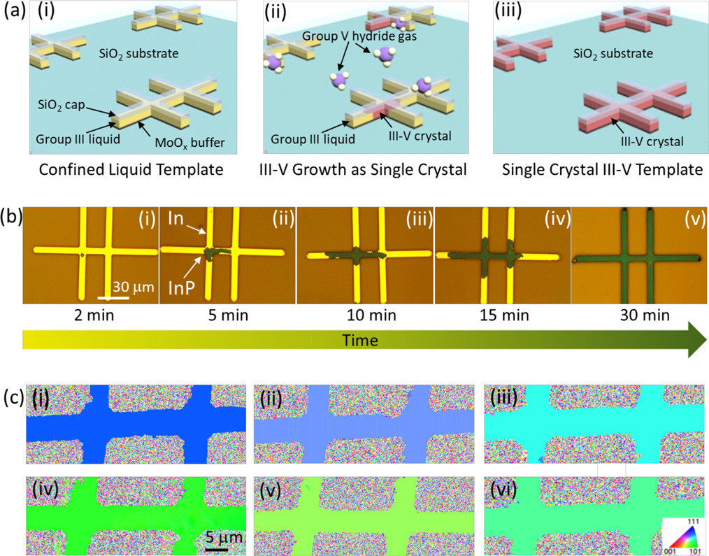
Figure 1: (a) Overview of large-area TLP growth. (b) (i)–(vi) Representative gray-scale optical microscope (OM) images of different stages of growth of InP in Hall-element geometry. (c) (i)–(vi) EBSD maps indicating single crystallinity.
Photoluminescence spectra obtained from TLP InP material showed a main peak at 1.34eV, which is the same as for commercial InP substrates. The full width at half maximum of the TLP material was only marginally larger than for commercial InP. The difference is described as “negligible” by the team.
Raman analysis of TLP InAs showed wavenumber shifts of 218.4/cm and 239.5/cm, corresponding to transverse (TO) and longitudinal (LO) optical phonon emissions in bulk InAs of 218/cm and 239/cm, respectively.
The technique was used to grow elements for Hall measurements. The initial indium layer was 225nm, which controlled the eventual In-V material thickness. The length and width of the structures were 100μm and 5μm, respectively.
The TLP growth was found to result in extraneous ‘side-growth’ of III-V material through a vapor phase process. This unwanted fuzz was removed using plasma etching, using the SiO2 cap as a mask. The etching thus reduced surface roughness scattering from the sidewalls in subsequent electron transport analysis.
The final preparation for van der Pauw Hall measurements was to remove the SiO2 cap, using wet or dry etching, and to deposit patterned annealed nickel/gold electrodes.
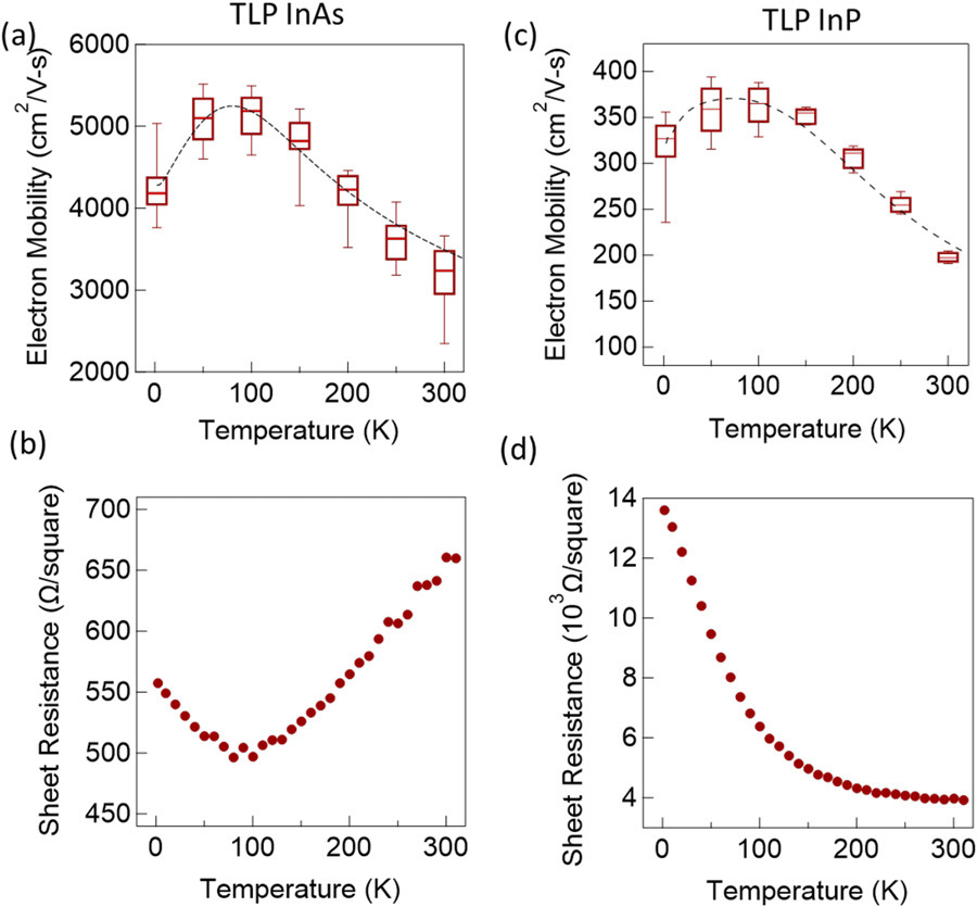
Figure 2: Hall mobility and sheet resistance of TLP InAs, (a, b, respectively) and InP (c, d).
The peak median mobility for InAs was registered around 100K at 5100cm2/V-s (Figure 2). The room-temperature (300K) result was a respectable 3200cm2/V-s. The peak at 100K is seen as being consistent with surface roughness scattering rather than a grain boundary impact on mobility, confirming the single-crystal nature of the material. A similar peak is found with epitaxially grown material.
The background carrier concentration was around 1x10¹⁷/cm3. The researchers used an electron-beam deposition process for the SiO2 cap, resulting in non-stoichiometric material with a silicon excess that could diffuse into the In-V crystal structure and provide unintentional n-type doping.
The mobility measurements for InP were lower with a peak of 370cm2/V-s at 100K, and 200cm2/V-s at 300K. The similarity in the curve shape is again seen as being limited by surface roughness scattering and indicative of single crystallinity.
The researchers comment: “Temperature-dependent mobility characteristics indicate that the grown materials are of comparable crystalline quality to that of epitaxially grown thin films. Importantly, this demonstration potentially opens up an avenue to integrate high-performance electronic and optoelectronic III–V devices on inexpensive amorphous substrates.”
InAs InP Amorphous silicon dioxide TLP
https://doi.org/10.1063/5.0006954
The author Mike Cooke is a freelance technology journalist who has worked in the semiconductor and advanced technology sectors since 1997.


