


News: Microelectronics
11 February 2021
HEMTs from AlScN-barrier MOCVD
Researchers in Germany and the Netherlands have used metal-organic chemical vapor deposition (MOCVD) to create aluminium scandium nitride (AlScN)-barrier high-electron-mobility transistors (HEMTs) [Christian Manz et al, Semicond. Sci. Technol., vol36, p034003, 2021]. The team also used silicon nitride (SiNx) cap material as an alternative to the more usual gallium nitride (GaN), which has never been investigated before, according the best knowledge of the team.
The work with AlScN builds on previous reports on MOCVD growth from the team at Fraunhofer Institute for Applied Solid State Physics (IAF), INATECH—Albert-Ludwigs Universität Freiburg, and University of Freiburg in Germany, and Eurofins Materials Science Netherlands and Eindhoven University of Technology in the Netherlands, along with Germany’s Fraunhofer Institute for Microstructure of Materials and Systems (IMWS) [www.semiconductor-today.com/news_items/2019/oct/fhg-iaf-281019.shtml].
The introduction of scandium into the barrier increases spontaneous and piezoelectric (strain-dependent) charge polarization, which enables up to 5x the sheet charge carrier density in the GaN two-dimensional electron gas (2DEG) channel on which HEMTs are based. GaN-channel HEMTs are being developed and deployed for high-power, high-voltage and high-frequency applications, ranging from electric vehicle (EV) and renewable energy power handling, to microwave wireless communications power transmission.
Although HEMTs have been fabricated before from molecular beam epitaxy (MBE)-grown AlScN material, MOCVD processes are more widely applicable for mass production. One problem with introducing scandium into MOCVD is that the vapor pressure of the potential precursors is low. The MOCVD was carried out at low pressure (40-100mbar) with hydrogen used as the carrier gas. The growth temperature ranged from 1000°C to 1200°C.
The nitrogen source was ammonia (NH3). The group-III metals, gallium and aluminium, came from trimethyl- (TM-) organics. The scandium precursor was tris-cyclopentadienyl-scandium (Cp3Sc). Silane (SiH4) supplied the silicon for the SiNx cap.
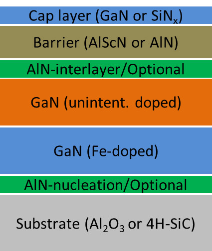
Figure 1: MOCVD scheme for AlScN barrier material.
The growth of the AlScN barrier layer used variously continuous and pulsed methodologies. The pulsed method consisted of alternating the metal supplies with 5s Cp3Sc and 2s TM-Al.
The experiments used 100mm sapphire substrates and 4H silicon carbide (SiC) for some experiments, particularly at the transistor fabrication stage.
The HEMTs consisted of titanium/aluminium ohmic source-drain contacts with ion-implant device isolation. The SiNx passivation enabled “low current dispersion and thermal stability”, according to the researchers. The gate was designed to be low capacitance, to improve high-speed operation.
The silicon nitride was used to cap the AlScN barrier layer, to avoid oxidation of the Al containing layer. In AlGaN transistors a GaN cap is often used, but in the case of AlScN such caps have been found to be difficult to grow, resulting in ‘3d islands’, which adversely impact its ability to protect and passivate the AlScN. GaN caps on AlScN were found to have root-mean-square roughness of 1.5nm for material grown at 1000°C, according to atomic force microscopy (AFM) measurements, compared with 0.2nm for SiNx.
The material used for the HEMTs (Figure 1) contained around 14% Sc in the 9.5nm AlScN barrier layer. The SiNx cap was 3.4nm. The growth temperature was 1100°C, with the AlScN deposition using continuous supply of the precursors. The substrate was 4H SiC. A comparison 5.6nm AlN barrier device with 3nm SiNx cap was also grown and fabricated.
Table 1: Comparison of electron transport properties of AlScN-barrier and AlN-barrier HEMTs.
| Barrier | AlScN | AlN |
| Sheet resistance | 323Ω/square | 325Ω/square |
| Mobility | 729cm2/V-s | 726cm2/V-s |
| Carrier concentration | 2.6x10¹³/cm2 | 2.6x10¹³/cm2 |
| Peak transconductance | 530mS/mm | 660mS/mm |
| Maximum drain current | 1720mA/mm | 1700mA/mm |
The HEMT with AlScN barrier achieved performance (Figure 2) comparable with that of the device with AlN barrier (Table 1). The researchers point out that the performance of the AlScN HEMT is below theoretical expectations.
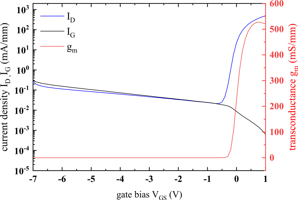
Figure 2: Transfer characteristics for AlScN-barrier HEMT with 0.25μm gate length. Drain bias 7V.
The team blames “heavy interdiffusion of the metal atoms Al, Ga and Sc in the buffer and barrier,” which was detected and characterized using scanning transmission electron microscopy (STEM), energy-dispersive x-ray spectroscopy (EDX), and high-resolution x-ray diffraction analysis (HR-XRD). The barriers were therefore AlGaScN and AlGaN, respectively. Measurements suggest that the diffusion resulted in an AlGaN barrier with around 40% Ga on average.
“The primary source for the lower mobility in both samples is most likely the poor interface quality and the atoms’ interdiffusion, causing alloy scattering, which is known to affect the mobility of HEMT heterostructures,” the researchers write.
Even so, the team sees the results as “very promising” for high-power and high-frequency applications, adding that the AlScN HEMT is “already superior” to standard AlGaN HEMTs designed for RF applications fabricated in-house.
HEMTs AlScN MOCVD GaN Sapphire substrates SiC
https://doi.org/10.1088/1361-6641/abd924
The author Mike Cooke is a freelance technology journalist who has worked in the semiconductor and advanced technology sectors since 1997.


