


News: Microelectronics
4 February 2021
Transistor cut-off frequency at 738GHz
A research team in Korea and Japan has reported field-effect transistors (FETs) with a cut-off frequency of 738GHz, claiming this as “the highest fT of any FET with any material system” [Hyeon-Bhin Jo et al, International Electron Devices Meeting, session 8.4, 2020].
The result from Kyoungpook National University (KNU), University of Ulsan and Quantum Semiconductor International Co Ltd in South Korea and NTT Device Technology Laboratories in Japan was presented online at the International Electron Devices Meeting (IEDM) at the end of 2020.
The team credits a composite indium gallium arsenide (InGaAs) quantum well (QW) channel structure with enabling the record frequency high-electron-mobility transistor (HEMT). The 738GHz figure compares with a previous InGaAs HEMT with 710GHz cut-off. However, the latter device also featured a maximum oscillation frequency (fmax) of more than 1THz (1000GHz), while the new device only achieved 492GHz.
The team sees renewed interest in InGaAs devices for future electronics, such as quantum computing and beyond-5G deployment, based on the potential for lower noise performance from the combination of high fT and low source resistance.
The researchers compared devices with a composite quantum well channel (Figure 1) with a more conventional In0.7Ga0.3As channel. The material was grown on 3-inch indium phosphide (InP) substrate. The buffer consisted of 200nm In0.52Al0.48As. The upper layers included a 3nm InP etch stop between the barrier and the heavily doped multi-layer cap.
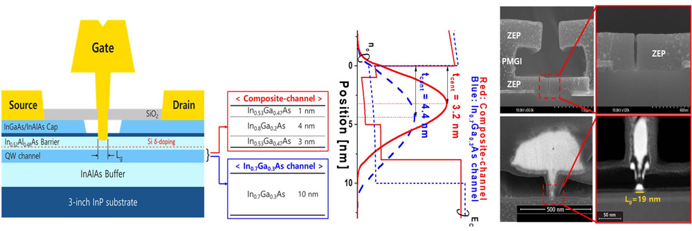
Figure 1: (a) HEMT schematic with two types of QW channel, (b) conduction-band profile in equilibrium under gate at 0.2V over threshold for both channel designs, and (c) cross-sectional scanning/transmission electron microscope (SEM/TEM) images of fabricated T-gate before and after gate metallization.
Hall-mobility measurements at a two-dimensional electron gas (2DEG) concentration of ~3x10¹²/cm2 showed an increase in mobility for the composite channel to 13,500cm2/V-s, compared with 10,500cm2/V-s for the more conventional channel. In the HEMT, the effective mobility was only slightly impacted at 13,200cm2/V-s; the average electron velocity under the gate was 6.2x107cm/s.
The fabricated HEMTs featured titanium/molybdenum/titanium/platinum/gold ohmic source/drain contacts scaled down to 0.8μm separation. Silicon dioxide (SiO2) was used in the fabrication of the recessed platinum/titanium/platinum/gold T-gate. The gate length (Lg) was as low as 19nm.
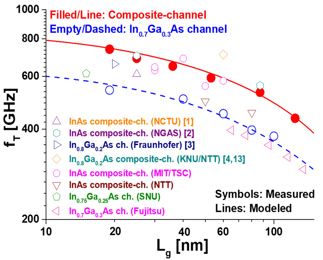
Figure 2: Benchmark of fT versus Lg for both devices against other reports.
The fT/fmax values were determined from measurements between 1 and 5 at 738GHz and 492GHz, respectively. The reference conventional-channel HEMT achieved corresponding values of 540GHz and 458GHz. The drain-source bias (VDS) was 0.5V.
The researchers comment: “To the best of our knowledge, the Lg = 19nm device with the composite channel produces the highest fT of any FET with any material system.” Combined with features such as an on-resistance of 271Ω-μm and 2.5μS/μm peak transconductance, the team adds that the device demonstrates “an outstanding combination of DC and high-frequency characteristics”.
The author Mike Cooke is a freelance technology journalist who has worked in the semiconductor and advanced technology sectors since 1997.


