


News: Microelectronics
25 February 2021
Flexible indium phosphide DHBT frequency boost
Southeast University and Nanjing Electronic Devices Institute in China have claimed the first demonstration of wafer-scale fabrication of high-frequency indium phosphide (InP) double heterostructure bipolar transistors (DHBTs) transferred to a flexible substrate [LiShu Wu et al, Semicond. Sci. Technol., vol36, p03LT02, 2021].
The team reports: “The cut-off frequency fT = 337GHz and maximum oscillation frequency fMAX = 485GHz are obtained, which represents the highest result ever reported in the field of flexible electronics to date.”
Flexible electronics is deployed is areas such as displays, solar cells, wearable electronics and bio-medical devices. Existing flexible electronics suffers from limited frequency performance, below the speed and bandwidth needed to access wireless communications/Internet of Things (IoT) technology. InP-based technology allows access to higher frequencies through much higher electron mobility.
Although new technologies such as graphene have enabled fT values of 198GHz (28.2GHz fMAX), the best flexible electronics performance previously was also achieved with InP, using high-electron-mobility transistor structures, achieving 160GHz fT and 290GHz fMAX.
The researchers contrast their wafer-scale achievement with previous reports, none of which “have yet been demonstrated to achieve high-performance flexible electronics at multi-gigahertz range on wafer scale, which will also limit the abroad application of RF flexible electronics.”
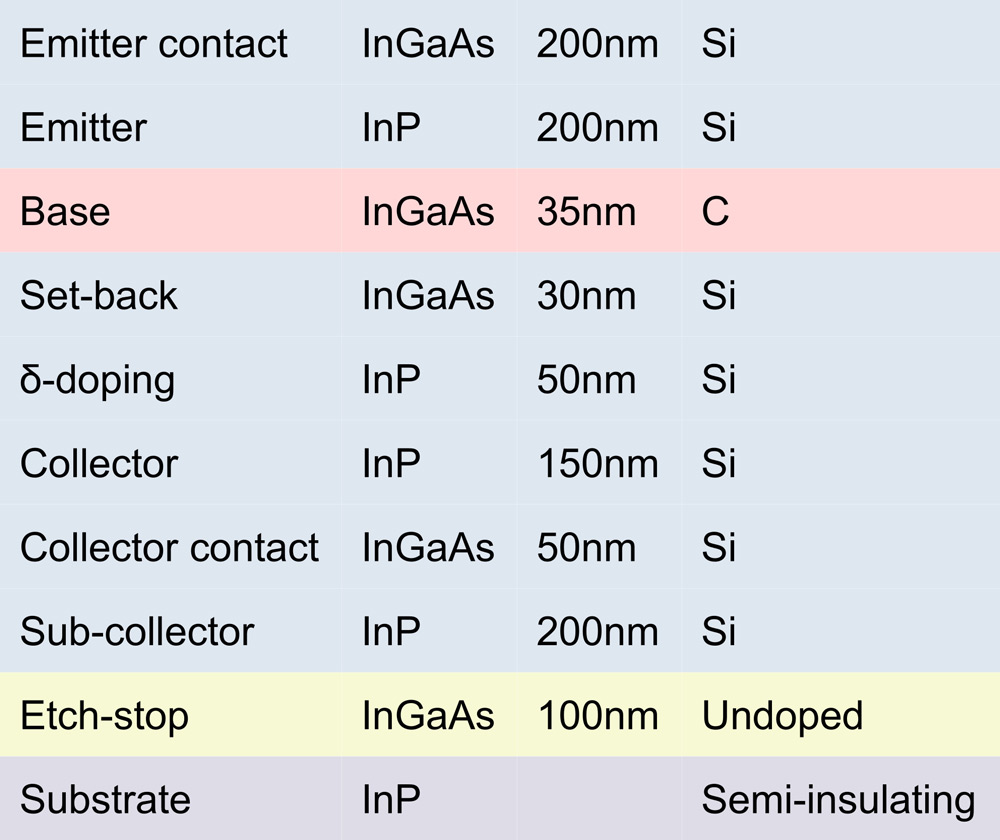
Figure 1: Layer structure of the InGaAs/InP DHBT.
The DBHT material was grown on 3-inch InP substrate using molecular beam epitaxy (MBE) – see Figure 1. The material was fabricated into single-finger DHBTs, using a 0.5μm process. Wet etching was used to define three stacked mesas for the DHBT, using self-aligned techniques to define the base contact. The emitter/collector metals were titanium/platinum/gold, and the base was platinum/titanium/platinum/gold. Further steps included device isolation, planarization/passivation with benzocyclobutene, reactive-ion etch to expose metal terminal posts, and pad deposition.
The transfer to flexible substrate involved temporary adhesion to sapphire carrier to enable removal/thinning of the InP substrate using mechanical lapping, followed by selective wet etching with a solution based on hydrochloric acid. The indium gallium arsenide (InGaAs) stop layer was removed with a solution based on orthophosphoric acid. The 2μm-thick device was then permanently bonded to the flexible substrate, and the sapphire carrier was removed.
DC measurements showed some degradation in performance in terms of collector current relative to devices not transferred to flexible substrates. The researchers attribute the degradation to poor thermal conductivity of the flexible substrate, about a factor of three lower than for InP. Self-heating can severely impact transistor performance. The maximum gain of 31 was only slightly impaired relative to the non-flexible devices.
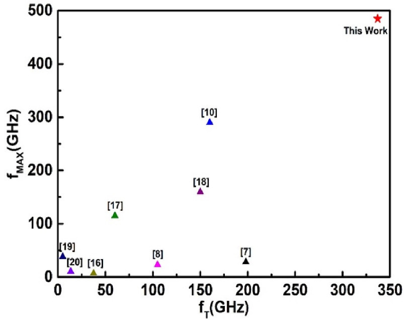
Figure 2: Comparison of fT/fMAX with previously reported semiconductor transistors on flexible substrate.
The frequency performance was measured up to 40GHz. A conventional DHBT achieved an extrapolated fT of 385GHZ with an fMAX of 570GHz. The DHBT on flexible substrate registered an fT of 337GHz and an fMAX of 485GHz. The researcher compared their work with other reports (Figure 2).
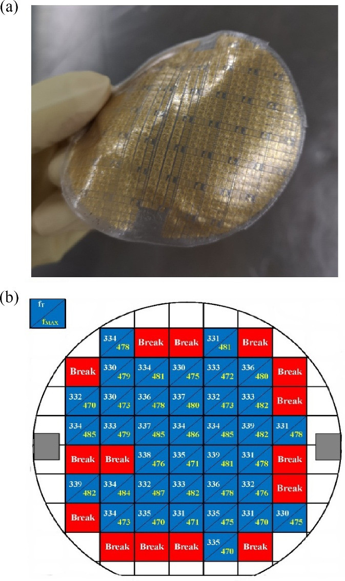
Figure 3: (a) Optical image of 3-inch InP DHBTs on flexible substrate. (b) fT/fMAX performance mapping under same measurement condition.
The process yield was around 73%, with most failed devices being on the periphery of the wafer (Figure 3). The failure was attributed to local defects. The frequency performance of the resulting devices varied only slightly.
InGaAs InP DHBTs InP substrates
https://doi.org/10.1088/1361-6641/abe05b
The author Mike Cooke is a freelance technology journalist who has worked in the semiconductor and advanced technology sectors since 1997.


