


News: LEDs
15 April 2021
Quantum dot powering up p-AlGaN
Researchers in China have improved the p-doping capability of magnesium in ultra-wide-bandgap (UWBG) aluminium gallium nitride (AlGaN) by incorporating quantum dot (QD) structures [Ke Jiang et al, Light: Science & Applications, vol10, p69, 2021]. The team from Changchun Institute of Optics, Fine Mechanics and Physics, together with University of Chinese Academy of Sciences, believes that the GaN QDs help to shift the valence-band maximum (VBM) closer to the Mg interband level (Figure 1), reducing the activation energy (Ea) by an order of magnitude and hence increasing the hole density.
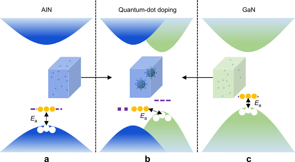
Figure 1: VB modulation to lower the acceptor Ea in UWBG nitrides. Acceptors randomly doped in (a) AlN and (c) GaN. (b) GaN QDs embedded in AlN matrix – acceptors in matrix concentrate near QD interface.
The researchers comment: “The quantum engineering doping method may also work in other UWBG semiconductors such as II–VI alloys, conductive oxides, or diamond because there are abundant heterostructures among their own congeners.” They see the technique as having implications for microelectronic and optoelectronic applications of AlGaN. As part of the work, they implemented the p-AlGaN:GaN QD structure in deep-ultraviolet light-emitting diodes (DUV-LEDs). On the pure electronic side, the availability of more effective p-doping could benefit efforts to produce high-voltage, high-frequency and high-power devices.
A test structure was grown by metal-organic chemical vapor deposition (MOCVD) on sapphire, using a non-equilibrium growth method. The buffer layers consisted of an AlN template and AlN/AlGaN superlattices to block dislocations.
The p-doped AlGaN:GaN QD system was realized using a non-equilibrium interrupt process. The AlGaN matrix resulted from simultaneous injection of trimethyl-Al and trimethyl-Ga, along with ammonia (NH3) and bis(cyclopentadienyl)-magnesium (Cp2Mg) for 10 seconds. The TMAl flow was then stopped for 10 seconds to grow the GaN QDs. The TMGa flow was then also stopped for 25 seconds to allow the QD structure to settle and encourage enriched Mg incorporation at the matrix-QD interface. The process was repeated around 40 times to give a 370nm p-AlGaN:GaN QD layer.
A post-deposition thermal anneal was used to activate the doping by driving out the hydrogen that tends to passivate the p-doping effect of Mg.
A high-angle annular dark-field scanning transmission electron microscope (HAADF-STEM) study found that the QDs were 2-3nm high and 6-8nm high. The Al content of the matrix was around 60%, according to secondary-ion mass spectroscopy (SIMS).
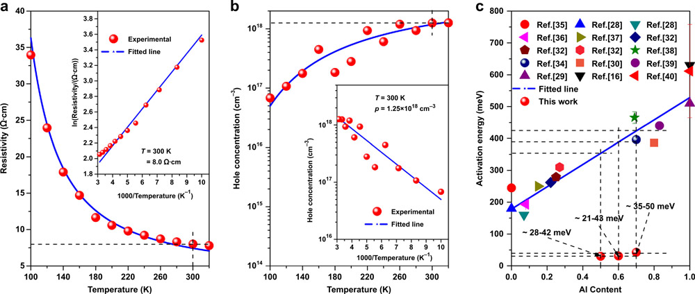
Figure 2: (a, b) Temperature-dependent resistivity and hole concentration from 100 to 320K. Inset: plots of reciprocal temperature (1000/T) versus log-scale resistivity and hole concentration. (c) Al-content-dependent Ea of Mg-doped disordered AlGaN alloys benchmarked against the new quantum engineering doped p-AlGaN:GaN QD structure (“this work”).
The resistivity of the material (Figure 2) was found to be 8.0Ω-cm at room temperature (300K). The activation energy for hole formation (derived from the temperature dependence of the resistivity) was 21meV, compared with ~400meV for p-AlGaN at 60% Al content. The hole concentration was put at 1.25x10¹⁸/cm3. The temperature dependence of this factor gave an activation energy estimate of 43meV.
Deep-ultraviolet light-emitting diodes were fabricated using the AlGaN:GaN QD p-doping. The current–voltage behavior showed improved current for a given voltage and higher light output, compared with a device using a standard p-AlGaN layer (Figure 3).
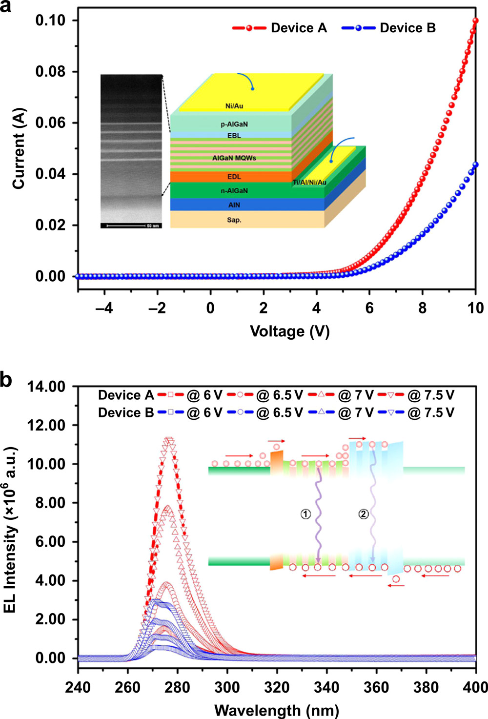
Figure 3: (a) Current–voltage behavior of DUV-LEDs with p-AlGaN:GaN QD (A) and uniform p-AlGaN (B). Inset: device structure and STEM image of active region. (b) EL spectra at different voltages. Inset: energy-band diagram of devices under bias.
The electroluminescence from the AlGaN:GaN QD LED red-shifted to longer wavelength under higher bias. The researchers attribute this to the quantum-confined Stark effect (QCSE) due to the higher electric field in the active region. By contrast, the uniformly doped p-AlGaN device saw little red-shift, which the team explains as being due to the lower potential drop across the active region. In the latter case, there is a larger potential drop across the more resistive p-AlGaN layer, compared with the p-AlGaN/GaN QD system.
Quantum dots p-AlGaN GaN QDs DUV-LEDs
https://doi.org/10.1038/s41377-021-00503-y
The author Mike Cooke is a freelance technology journalist who has worked in the semiconductor and advanced technology sectors since 1997.


