


News: Suppliers
15 April 2021
II-VI expands conductive SiC wafer finishing capacity in China
Engineered materials and optoelectronic component maker II-VI Inc of Saxonburg, PA, USA has expanded its silicon carbide (SiC) wafer finishing manufacturing footprint in China to serve the world’s largest market for electric vehicles (EVs) and for clean energy applications.
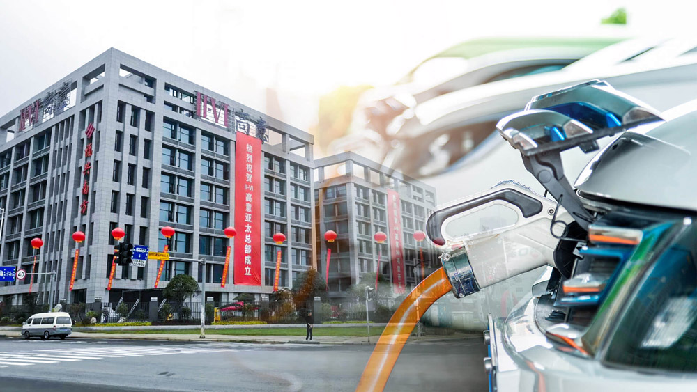
Spurred by increasing regulatory requirements for lower emissions of greenhouse gases and the decreasing cost of lithium-ion batteries, the market for EVs is growing rapidly and driving demand for power electronics based on silicon carbide which, as a wide-bandgap semiconducting material, can boost the driving range of EVs by about 10% on a single charge, compared with power electronics based on silicon. To meet the market demand in Asia, II-VI has established a backend processing line for conductive SiC substrates, in over 50,000ft2 of new cleanroom space, at II-VI’s Asia Regional Headquarters in Fuzhou, China.
“According to recent industry reports, China is expected to continue to be the world’s largest electric car market, at over 40% of global sales,” says Sohail Khan, executive VP of II-VI’s New Ventures & Wide-Bandgap Electronics Technologies business unit. “We are planning to substantially increase our global production capacity for SiC boules and substrates in the US over the next 5-10 years to address the accelerating power electronics market, including for electric vehicles and clean-energy applications,” he adds. “These investments will be supported by our global sales force and a SiC platform built by our innovations of the last 20 years, including the world’s first 200mm conductive substrates in 2015.”
In addition to EVs, power electronics based on SiC enable high efficiency in inverters for solar and wind energy generation, as well as in smart-grid power switching, due to reduced switching losses, high power density, better heat dissipation and increased bandwidth capability compared with existing devices based on silicon.
The backend SiC wafer processing performed at II-VI’s new SiC facility in Fuzhou includes edge grinding, chemical-mechanical polishing (CMP), cleaning and inspection, all performed in Class 100 and 1000 cleanrooms. The facility is part of II-VI’s already announced plan to ramp its SiC substrate manufacturing capacity by 5-10 times over five years, including with 200mm diameter substrates. II-VI maintains a large manufacturing operations and product development presence in China in the cities of Fuzhou, Guangzhou, Shanghai, Shenzhen, Suzhou, and Wuxi.
II-VI completes Ascatron and INNOViON acquisitions, and joins SIA


