


News: Microelectronics
1 April 2021
III-V resonant tunneling for ULTRARAM
UK-based researchers report the first tests of an ‘ULTRARAM’ III-V memory that incorporates quantum resonant tunneling as part of its operation “to achieve non-volatility at extremely low switching energy per unit area” [D. Lane et al, IEEE Transactions on Electron Devices, published online 25 March 2021].
The team from Lancaster University, University of Liverpool and University of Warwick hopes that the technology could form the basis for a ‘universal memory’, combining the speed and random-access advantages of dynamic random access memory (DRAM) and the non-volatility of Flash. The universal-memory dream is discounted by most researchers as being “unfeasible or almost impossible”.
The UK team believes that the “unusual band offsets” of the ‘6.1Å’ lattice-spacing family of high-mobility III-V materials – indium arsenide (InAs), aluminium antimonide (AlSb) and gallium antimonide (GaSb) – offer hope in this regard. The researchers write: “In particular, the extraordinarily large conduction-band offset of InAs/AlSb (2.1eV) delivers electron barriers akin to those of dielectrics to achieve non-volatility.”
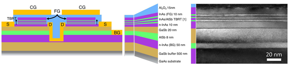
Figure 1: Left: cross-sectional schematic of ULTRARAM and material layers. Right: dark-field transmission electron microscope image of epitaxial structure.
The material structure for the ULTRARAM was grown on 2-inch heavily doped n-type GaAs substrates, using molecular beam epitaxy (MBE). The lattice mismatch between GaSb and GaAs is 7.8%. An interfacial misfit array between the GaAs and GaSb buffer was used to mitigate the problems that can arise from the relatively large difference in lattice parameter. The active part of the memory element was provided by GaSb/InAs/AlSb layers.
The triple-barrier resonant tunneling (TBRT) structure consisted of alternating InAs/AlSb layers. The InAs/AlSb provides a 2.1eV barrier to charge leakage from the InAs floating gate (FG) structure at low bias. However, the resonant tunneling allows electrons to enter and leave the FG easily with an applied bias of about 2.5V. This voltage is about a factor of ten lower than that needed in Flash memory program/erase operations.
The fabrication used a combination of alternative inductively coupled plasma (ICP) and selective wet etching. The plasma etch was controlled using in-situ reflectance measurements. The plasma source gases were boron trichloride, chlorine and argon. The wet etching variously used tetramethylammonium hydroxide (AlSb and GaSb) and a citric acid/hydrogen peroxide solution in water (InAs).
The drain/back gate/drain (D/BG/D) and source (S) contacts were sputtered titanium/gold. The control gate (CG) stack consisted of atomic layer deposition (ALD) aluminium oxide (Al2O3) and the CG metal. The Al2O3 was used to reduce current flow during operation, which adversely impacts device efficiency. The Al2O3 presents a 3.1eV barrier to charge leakage from the InAs floating gate. Passivation was provided by plasma-enhanced chemical vapor deposition (PECVD) silicon dioxide (SiO2).
Buffered oxide etching was used to reveal the various contacts and then titanium/gold pads were applied. The metallization also included the formation of word-lines connecting the CGs and bit-lines linking the S-terminals.
The gate length of the devices was 20μm. The devices were fabricated in 2x2 arrays. The program (P) and erase (E) cycles, at -2.5V and +2.5V, respectively, lasted 500μs. The team comments: “Such a P/E cycle corresponds to a 102 and 103 reduction in switching energy per unit area compared to DRAM and NAND flash, respectively.”
The P/E cycle was 2000x faster than the group’s previous devices. The researchers suggest that smaller devices with gate lengths of the order of 20nm could perform at sub-nanosecond rates: “significantly faster than DRAM and comparable to static RAM (SRAM)”. However, this would need to be confirmed in actual devices, rather than through assuming ideal scaling.
It was found that the 2.5V P/E biasing could be applied in various ways, e.g. grounding the word-line while biasing the bit-line, or applying opposite 1.25V biases to the word- and bit-lines.
The current flow contrast between the 1 and 0 states is presently a concern if 1000s of cells were to be connected to the bit-line. The relatively small difference was attributed to the use of n-InAs as the channel, which tends to be ‘normally-ON’, and the ‘OFF’ state is achieved with partial depletion of the channel by charges in the floating gate structure. The team reports: “Work is ongoing to incorporate the normally-OFF InGaAs channel design described in our previous work to address this issue.”
Reliability studies carried out on one memory element showed stable current contrast between the states over 8x10⁵ readout cycles, involving 0.5V SD bias. In a test with 106 5ms P/E switching cycles performed at a rate of 200/minute, the 0/1 contrast was successfully maintained (Figure 2).
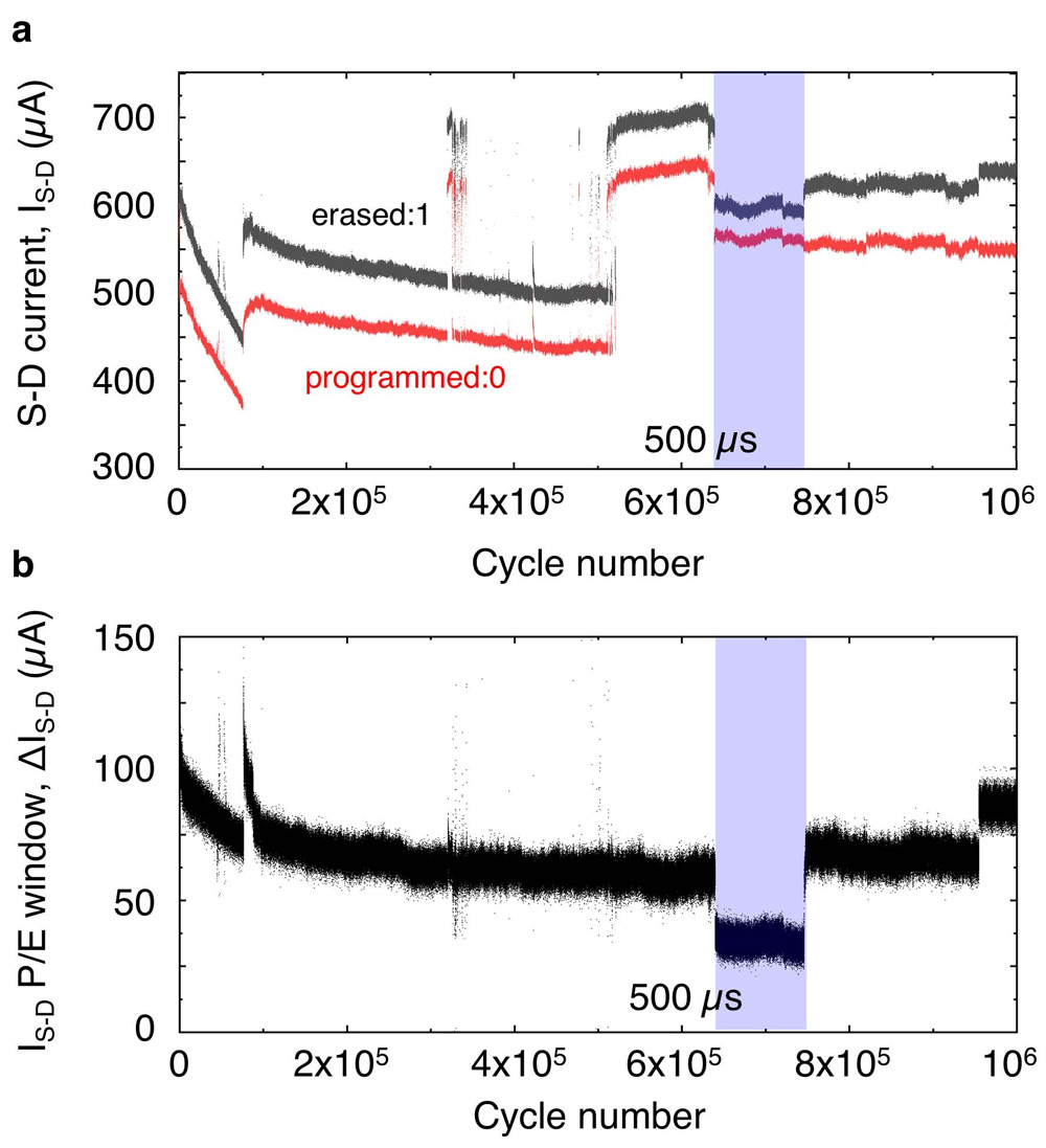
Figure 2: Memory cell endurance data: (a) S-D current after +2.5V erase cycle (gray), and −2.5V program cycle (red). Pulse duration 5ms, except for blue shaded region where 500μs pulse duration was used. (b) S-D current difference calculated by subtracting erase and program current from consecutive cycles.
Shorter P/E cycles (500μs) suffered from reduced contrast (blue-shaded region in Figure 2), the problem being resistance-capacitance (RC) delays rather than the extremely fast tunneling mechanism. The delay means that the bias does not reach the desired 2.5V within the shortened cycle. Presumably, reduced feature sizes would speed up the devices through reducing parasitic capacitance.
The researchers comment: “In this first-ever test, endurance is at least an order of magnitude higher than flash memory.”
The researchers are not sure of the cause of shifts of the 0/1 window within the time-span of the test. They suggest it could be due to “an inconsistent channel contact that is sensitive to temperature or vibrations”. Visual evidence for this hypothesis came in the form of atomic force microscopy (AFM) scans showing etch pits in the channel surface, which could create inconsistent contacts. The team reports: “An ICP etch process to create a smooth surface for consistent contact to the thin (10nm) channel material is currently being developed in response.”
materials – InAs AlSb GaSb MBE PECVD
https://doi.org/10.1109/TED.2021.3064788
The author Mike Cooke is a freelance technology journalist who has worked in the semiconductor and advanced technology sectors since 1997.


