


News: Microelectronics
5 August 2021
GaN complementary logic platform
Hong Kong University of Science and Technology (HKUST) and Peking University in China have reported progress in producing gallium nitride (GaN) complementary logic (CL) circuits on low-cost silicon [Zheyang Zheng et al, Nature Electronics, published online 19 July 2021].
The operation of the circuits was similar to that achieved with silicon complementary metal-oxide-semiconductor (MOS) p- and n-type transistors (CMOS). However, the GaN complementary logic circuits were based on a MOS p-FET, but an n-type heterojunction field-effect transistor (n-HFET) with a p-GaN gate electrode. A key property of these devices was that they operated in ‘enhancement-mode’ with current blocking at 0V gate potential – i.e. ‘normally-off’ operation.
The researchers see potential uses in the control of circuits for power electronics, radio-frequency power amplifiers and harsh-environment applications. The team comments: “The desire of monolithically integrating peripheral circuits with GaN power switches that operate at intermediate frequencies offers a compelling yet relaxed opportunity for GaN complementary logic circuits. The typical operating frequencies are in the range of 100kHz to 10MHz, technically reachable for GaN CL circuits within acceptable costs.”
The researchers used commercial GaN on silicon (Si) wafers grown by metal-organic chemical vapor deposition (MOCVD). The layer structure on the p-Si wafer was 4μm GaN transition/buffer, 12nm aluminium gallium nitride (AlGaN) buffer, and 85nm p-GaN. Hall measurements on the material suggest a sheet hole density of 1.23x10¹³/cm2 with 10.2cm2/V-s mobility. The mobility is within the range of material specifically designed to create p-FETs (~15cm2/V-s), rather than an off-the-shelf product aimed at power GaN n-FET applications.
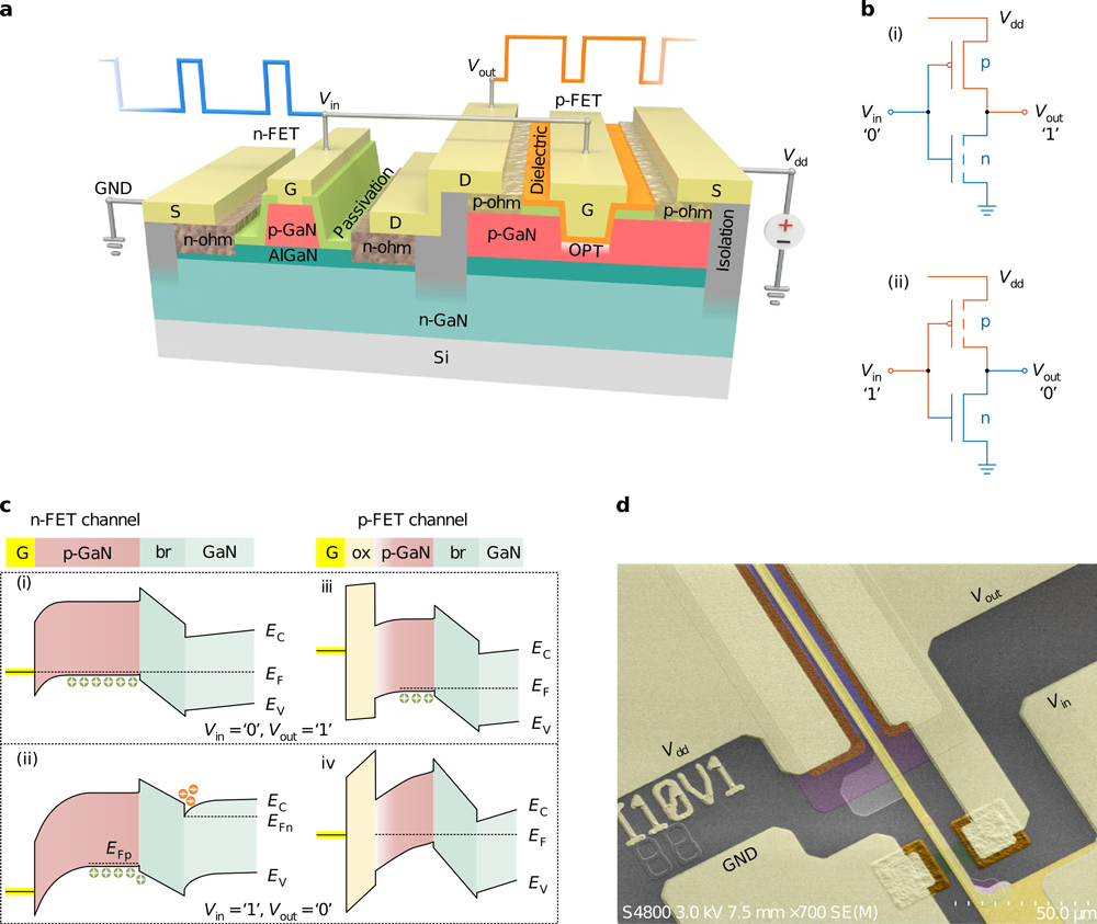
Figure 1: a, Schematic GaN complementary logic inverter. b, Schematic CL inverter circuit at two static logic states. c, Schematic energy band diagrams under different logic inputs. d, Scanning electron micrograph in false color.
The first fabrication step was the removal of p-GaN using plasma etching, leaving the p-GaN gate of the n-FET and material for the p-FET (Figure 1). Next, a 70nm silicon dioxide surface passivation layer was deposited. The ohmic source/drain contacts of the n-FETs were formed by opening windows in the passivation and evaporating titanium/aluminium/nickel/gold, followed by 850°C rapid thermal annealing (RTA) for half a minute. The p-FET ohmic contacts consisted of nickel/gold, annealed at 550°C in oxygen for 10 minutes.
The p-FET channel was formed by inductively coupled plasma (ICP) reactive ion etch of a trench, leaving 30nm of p-GaN material for the channel.
The desired enhancement-mode behavior for the p-FETs was realized using a one-minute oxygen plasma treatment of the p-channel surface by depleting holes through a shift of the valence band maximum away from the Fermi level with the formation of oxygen complexes with and/or passivation of the magnesium doping.
The p-FET gate insulation consisted of 20nm aluminium oxide (Al2O3). The plasma treatment resulted in a buried p-channel, which conducts holes away from the gate dielectric interface, reducing carrier scattering and disorder effects that increase electrical resistance.
The devices were isolated using fluorine ion implantation rather than mesa etch, avoiding current leakage through sidewall conduction. The gate electrodes and probe pads consisted of nickel/gold. The metal of the p-GaN gate of the n-FET formed a Schottky contact. The p-GaN enables enhancement-mode operation for the n-FET.
To balance the performance of the n- and p-FETs for complementary logic, the width of the p-FET was around 10x that of the n-FET. In specific measurements, the n-FET was 10μm wide and the p-FET 100μm. Other dimensions were: for the n-FET, 2μm gate-to-source, 3.5μm gate length, and 2μm gate-to-drain; corresponding dimensions for the p-FET were 3μm, 1.5μm, and 3μm.
The performance of the basic complementary logic inverter circuit is described as ‘rail-to-rail’, with the 1-state output being equal to the supply voltage and the 0-state being ground. With the supply between 3V and 5V, a sharp transition from the 1-state to the 0-state occurs when the input reaches around half the supply voltage. However, with 2V supply there is an intermediate state with both of the FETs in the off-state when the input is ~1V. The voltage gain in the transition region for 5V-supply reached 80V/V.
Due to large on/off current ratios ~107, the static power dissipation is suppressed. The researchers comment: “This inverter unambiguously demonstrates the most important trait of CMOS circuits, that is, low static-state power dissipation, and thereby outperforms other logic circuit schemes, such as resistor–transistor logic or directly coupled FET logic (DCFL) structure, in terms of energy efficiency.”
A 5V supply is commonly available for logic control sub-circuits of GaN power electronic systems. The noise margins were found to be 2.1V for the low state, and 2.6V for the high state. “Both noise margins are sufficiently large; therefore GaN complementary logic devices are equipped with high immunity to miscellaneous noises, such as electromagnetic interferences produced by high-frequency power switches,” the team writes.
The researchers also subjected the inverter circuit to increased temperatures. “Despite a slight expansion in the transition window and deviations in VTH at high temperatures, superior properties of the GaN complementary logic inverter, such as rail-to-rail operation, wide noise margins and sharp logic state transition, are well preserved,” the team observes of measurements made at 200°C. Even at 350°C, the noise margins were 1.83V and the voltage gain reached 18.10V/V. Silicon circuits suffer increasing degradation problems beyond 125°C such as latch-up and other malfunctions from thermally induced leakage.
The p-FET performance was the limiting factor for continuous switching up to 2MHz. The researchers hope that further optimization of the channel recess etch and oxidation process will lead to devices capable of several MHz performance. Another potential booster would be scaled reduction of the device size with gate lengths as small at 180nm, although 250nm would probably be more realistic in terms of avoiding short-channel effects.
More complicated circuits such as NAND, NOR, and transmission (a CMOS-like switch) gates were fabricated. The researchers report: “The demonstration of a complete set of elementary complementary logic gates indicates that the n–p integration technology is a feasible approach to construct complicated combinational GaN complementary logic circuits.”
Further demonstrations of multi-stage integration came in the form of a latch circuit and a ring oscillator. The latch consisted of cross-coupled inverters, giving a 1-bit memory storage. The researchers comment: “The capability of storing data enables the implementation of memory units (for example, static random-access memory) and sequential logic circuits. Therefore, it becomes feasible to construct finite-state machines or microprocessors using GaN.”
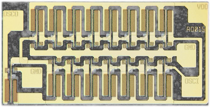
Figure 2: Confocal laser microscopy photograph of ring oscillator.
The ring oscillator (Figure 2) consisted of 15 cascaded inverter and a 1-inverter output buffer. The oscillating period was 1.99μs and the fundamental frequency was 502kHz.
GaN CMOS AlGaN MOS p-FET n-HFET MOCVD
https://doi.org/10.1038/s41928-021-00611-y
The author Mike Cooke is a freelance technology journalist who has worked in the semiconductor and advanced technology sectors since 1997.


