


News: LEDs
12 August 2021
MOCVD tunnel junctions beat ITO for blue μLEDs
University of California Santa Barbara (UCSB) has demonstrated micro-scale blue light-emitting diodes (μLEDs) with metal-organic chemical vapor deposition (MOCVD) tunnel junction (TJ) contacts with peak external quantum efficiency (EQE) and wall-plug efficiency (WPE) significantly higher than devices using indium tin oxide (ITO) [Matthew S. Wong et al, Appl. Phys. Express, vol14, p086502, 2021].
UCSB has been developing MOCVD GaN TJs for some time. In July, we reported on UCSB’s work in using MOCVD TJs to stack blue and green LEDs [www.semiconductor-today.com].
A key problem with TJ contacts in indium gallium nitride (GaN) LEDs is that the p-side of the device becomes buried under n-GaN material. This makes it difficult to activate the magnesium doping that provides acceptor levels that grab electrons out of the valence band, creating mobile positively-charged holes in the p-GaN layers.
The activation of p-GaN is mainly designed to drive out hydrogen, which passivates the magnesium acceptor states, blocking the desired generation of holes. This is normally achieved with thermal annealing. However, if the p-GaN is buried, it becomes much more difficult to activate the doping.
With μLEDs there is a potential escape route for the hydrogen through the sidewalls of the device but, as we will see, this route can be blocked by damage from the etch used to create the device mesa. The UCSB team implemented a chemical treatment to open up this hydrogen escape path.
An alternative technique to achieve TJs is to use molecular beam epitaxy (MBE), where the presence of hydrogen can be avoided. However, MBE is generally slower than MOCVD so, in industrial contexts, the latter process is preferred.
However, μLEDs are not just a useful way to allow the use of more transparent n-GaN as a current-spreading contact on p-GaN instead of ITO. Such devices are being explored for deployment in next-generation display and visible-light communication systems. The UCSB researchers comment: “Monolithic III-nitride-based μLEDs are particularly interesting for near-eye display applications, since this approach will simplify the mass transfer process with high pixel-per-inch standards.”
The UCSB team used commercial blue LED wafers grown on sapphire through MOCVD. The peak wavelength was designed to be 465nm at 20A/cm2 current density.
The TJ was created using three added n-type layers: 10nm n++-GaN, 100nm n-GaN, and 10nm n+-GaN. The MOCVD growth temperatures were 825°C for the first layer, and 900°C for the others. The commercial wafers were prepared for the TJ growth step with a 5-minute buffered hydrofluoric acid (BHF) dip.
The μLEDs were fabricated with the mesas formed using reactive-ion plasma etch. The mesa areas ranged from 5μmx5μm to 100μmx100μm.
A chemical treatment was performed before activation of the buried p-GaN, consisting of a series of cycles of 5-minute treatments: 60° phosphoric acid treatment, ultraviolet-ozone, and BHF dip. The p-GaN activation was 30 minutes 700°C annealing in a nitrogen/oxygen environment.
The researchers see the chemical treatment as reducing the sidewall damage from the mesa plasma etch. The damage creates band-bending effects, which can result in mid-level defects and regions of n-type material near the sidewall surface of the p-GaN.
The surface damage creates a barrier to the diffusion of hydrogen out of the p-GaN sidewalls during thermal annealing. For example, the preferred states of hydrogen is H+ in p-GaN, and H- in n-GaN. The H+ ions are therefore blocked from entering n-GaN regions.
Scanning electron microscope (SEM) studies showed that, without chemical treatment, the sidewalls appeared to be smooth (Figure 1). The chemical treatment made for rougher, but more vertical sidewalls.
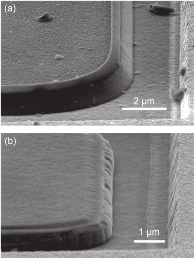
Figure 1: SEM images of μLED sidewall profiles (a) without and (b) with chemical treatments.
A dielectric isolation layer of 3x silicon dioxide/tantalum pentoxide pairs, capped with aluminium oxide, also served as an omnidirectional reflector (ODR). Further silicon dioxide deposition provided mesa sidewall passivation.
The devices were completed with opening contact windows in the dielectric with BHF etch, followed by deposition of the aluminium/nickel/gold electrodes. Reference devices were also produced with 110nm ITO on the p-GaN rather than a tunnel junction.
Electrically the chemical treatments reduced the forward voltage needed to generate a given current injection. The greatest improvement was achieved in one cycle. The optimal voltage reduction was given by three cycles. The increased resistance from further cycles was attributed to formation of an n-type diffusion barrier due to oxidation.
The team explains: “The additional number of chemical treatment cycles provides oxygen at the sidewalls, where oxygen acts as a donor in the p-GaN and converts to n-type, and hence immoderate use of chemical treatments would result in more resistive characteristic than the optimal condition.”
There was also a size penalty with larger devices being more resistant to current flow, suggesting incomplete p-GaN activation. The team writes: “Because this proposed method relies on sidewall activation, this method is effective to device dimensions less than 40μm, yet additional activation is needed to utilize this method on devices with larger area.”
The forward voltage on a 20μmx20μm device at 20A/cm2 was 5.3V without chemical treatment, and 3.05V with a 3-cycle treatment. A reference device with ITO transparent current-spreading layer on the p-GaN had a 2.85V forward voltage at 20A/cm2. The 0.2V penalty between the 3-cycle TJ and ITO is lower than that achieved with MBE for TJs.
The benefit of the TJ over ITO is that it is more transparent to the emitted blue light. The light output power was greater in both TJ devices relative to ITO for a given current injection.
At 20A/cm2 injection, the light output power was 42% and 46% greater than the ITO device, for the TJ without and with chemical treatment, respectively. The corresponding improvements were 15% and 30% at 60A/cm2 injection. The faster fall off in performance of the TJ device at higher currents was attributed to increased Joule heating from the higher voltages needed.
The balance between energy loss, as expressed through higher forward voltage, and light output power was determined through external quantum efficiency (EQE) and wall-plug efficiency (WPE) – see Figure 2. The device with ITO contact achieved peak EQE and WPE of 34% and 31%, respectively. The corresponding figures for the chemically treated TJ μLED were 56% and 55%. As the current increased, the TJ μLED demonstrated ~10% higher EQE over the ITO-contact device. For the WPE, the TJ value descended to the ITO level at higher current injection.
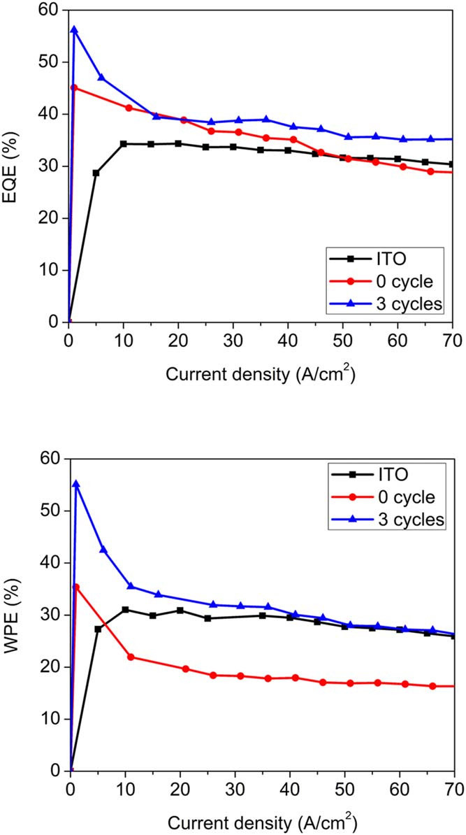
Figure 2: (top) EQE and (bottom) WPE of 20μmx20μm devices with ITO or TJ contacts.
The researchers comment: “The higher WPE performance at low current density was attributed to the greater light output power (LOP), where the voltage penalty was relatively low and the enhancement in LOP was significant, and the increase in WPE diminished with current density.”
MOCVD tunnel junctions MOCVD ITO Blue μLEDs GaN
https://doi.org/10.35848/1882-0786/ac1230
The author Mike Cooke is a freelance technology journalist who has worked in the semiconductor and advanced technology sectors since 1997.


