News: Optoelectronics
2 December 2021
Slow-light VCSEL power boost
Researchers based in Japan and Egypt claim record single-mode power of more than 5W for a high-power single-mode vertical-cavity surface-emitting laser (VCSEL) with a slow light mode (SLM) surface grating [Ahmed M. A. Hassan et al, Appl. Phys. Lett., v119, p191103, 2021].
The team from Tokyo Institute of Technology in Japan, Al-Azhar University in Assuit, Egypt, Ambition Photonics Inc in Japan, the National Institute of Information and Communications Technology in Japan, and Minia University in Egypt see the potential for high-power applications including 3D sensing of objects in light detection and ranging (LIDAR) and structured light 3D scanning, which analyses the deformation of projected patterns to extract depth and surface information.
The researchers comment: “Unlike long-cavity in-plane edge-emitting lasers, an SLM-based VCSEL can provide higher output powers without limitation of catastrophic optical mirror damage.”
Normal VCSELs are limited in output power to the milliWatt level due to their small volume. High output power is gained at the expense of beam quality. The SLM in the researchers’ device is propagated laterally at a wavelength near the resonant/cut-off frequency where there is a large degree of dispersion between the frequency and wavelength, leading to the slow light effect in terms of the group velocity.
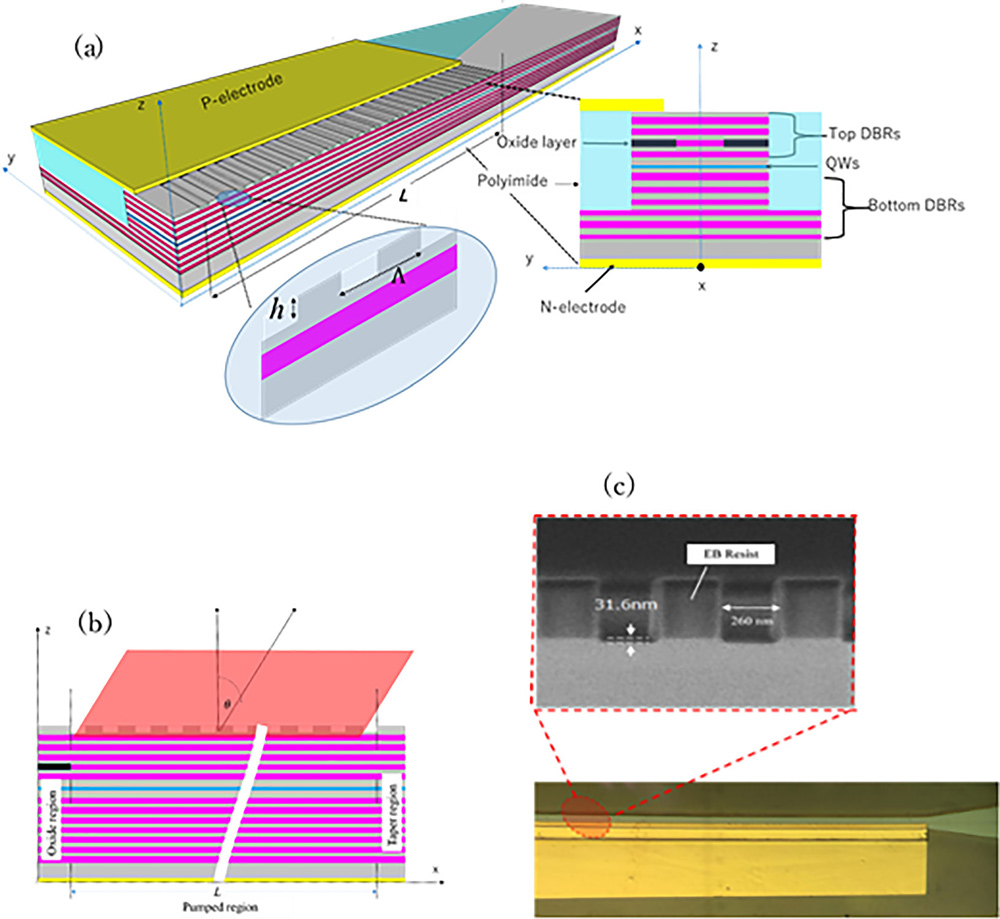
The VCSEL part of the device was an ~850nm wavelength gallium aluminium arsenide (GaAlAs) structure with three GaAs quantum wells and GaAs/GaAlAs distributed Bragg reflectors (DBRs) on each side (Figure 1). A surface grating was added on the top p-side 19-pair DBR of the device to give the SLM, which was detuned 20nm shorter than the vertical-cavity resonance wavelength. The researchers comment: “This detuning design gives a higher gain and, hence, lower threshold current for the SLM than a vertical lasing mode.” The pitch of the grating was as large as 0.5μm, making fabrication fairly easy, using electron-beam lithography and dry etch.

Figure 1: Structure and emission mode of device. (a) Schematic structure of surface grating VCSELs, top view and cross-section. (b) Side cross section showing radiation of slow light at angle (θ). (c) Microscopic photo of real device showing surface gratings.
The tapered rectangular device mesa was 4.5μm high and 34μm wide. Wet oxidation was used for lateral optical confinement. Oxide regions were also used to confine the injection current. Polyimide was used for planarization. The taper section was 500μm long with a taper angle of 10°, which was found to have less than 0.5% back reflection, suppressing Fabry-Perot modes. The other end of the lateral laser cavity at the semiconductor/oxide interface was highly reflective.
The device had a rectangular beam shape. “This kind of beam could be suitable for LIDAR systems and structured light sensing,” the team writes. The researchers envisage devices on the scale of millimeters or even centimeters, which would increase the output power proportionally. They add: “Because the output power could be increased by increasing the device length even with keeping the surface power density and the active region is not exposed to air, catastrophic optical mirror damage can be totally avoided.”
A 1mm-long device achieved lasing at 50mA injection under pulsed-mode with 50ns pulses to avoid self-heating, and a 2mm laser at 120mA. The slope efficiency for both devices was 0.59W/A. The maximum output powers were 180mW and 280mW, respectively. The devices suffered from thermal rollover, since there was no heatsink.
In continuous wave (CW) operation, the side-mode suppression ratio (SMSR) was more than 30dB. The single-mode wavelength of the 1mm device was 830.8nm at 100mA injection, close to the 830nm design target. At higher currents there was a thermal red-shift to 833.6nm at 350mA. A 845.4nm vertical lasing mode appeared at 300mA. The team comments: “At this current, the gain aligned into vertical modes. It is important to eliminate the lasing of vertical modes to boost the output of a single slow light mode at high currents.”
The researchers suggest that the ~3nm red-shift could see application in integrated beam scanners.
The far-field pattern showed a very low beam divergence of 0.084° at 100mA, around 2x the threshold for the 1mm device. The divergence increased at higher currents to 0.2° at 250mA injection, but narrowed somewhat to 0.18° by 300mA. The longer 2mm device had a narrower beam: ~0.056° at 170mA, reducing slightly to 0.053° at 300mA.
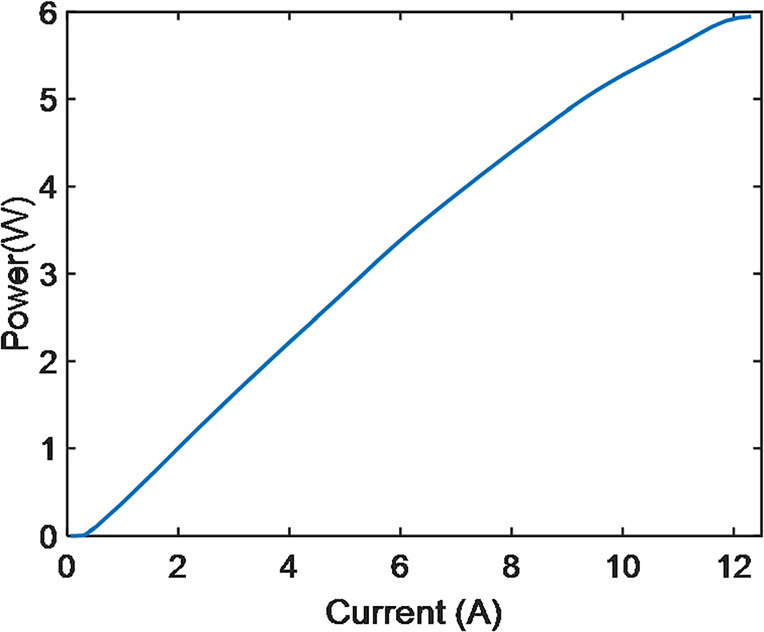
A 6mm-long device with 4μm wide oxide aperture achieved a stable single mode at 833nm with 30dB SMSR at 1A CW injection. The beam divergence was 0.19° at 1A with a minimum 0.038° at 350mA. A peak output power of 6W at 12A was achieved under pulsed operation with 50ns pulses and 1ms repetition (Figure 2). The slope efficiency was 0.6W/A. The power output saturated around 10A due to self-heating and current non-uniformity in the long device. The avoidance of self-heating in pulsed operation allowed a reduced beam divergence of 0.12° at 1A. At 12A, the divergence was 0.25°.

Figure 2: Light output power-current curve of 6mm device under 50ns pulsed operation.
The researchers comment: “All of the measurements were done by using a single current probe, which causes non-uniform current distribution in particular, for long devices at high current injection. We expect significant improvements in the output power and reduction of beam divergence if wire and die bonding is carried out with better thermal management.”
VCSEL LIDAR GaAlAs GaAs quantum wells DBRs
https://doi.org/10.1063/5.0066590
The author Mike Cooke is a freelance technology journalist who has worked in the semiconductor and advanced technology sectors since 1997.


