


News: Optoelectronics
9 December 2021
GeSn-on-insulator platform for lasing
Université Paris-Saclay and Université Côte d’Azur in France have reported work on germanium tin on insulator (GeSnOI) laser structures [Binbin Wang et al, Light: Science & Applications, vol10, p232, 2021].
The team comments: “The key advantage of this GeSnOI platform is its ability to combine active laser structures with passive SiN circuitry from the near-infrared to the mid-infrared. It represents a new paradigm for infrared Group-IV photonics that eliminates the need for III–V laser integration.”
Being a group-IV compound/alloy, GeSn is easier to integrate with the mainstream (group-IV) silicon (Si) complementary metal-oxide-semiconductor (CMOS) manufacturing infrastructure that powers the modern world. Band and strain engineering of GeSn has led to hopes of efficient light emission through direct-bandgap transitions, as opposed to the generally non-radiative indirect bandgaps of Si and pure Ge.
Although the reported devices with 10.5% Sn content only operated at cryogenic temperatures below 140K, the researchers believe that, with higher Sn content, lasing around room temperature could be achieved. GeSn with 16% Sn has been used to demonstrate lasing in suspended structures at 270K, just below 0°C. The higher tin content improves the directness of the bandgap.
The GeSn bandgap is relatively narrow, coming in the mid-infrared range where applications in biochemical detection, gas monitoring and thermal imaging suggest potential. The team also believes that its GeSnOI platform could support electrically pumped devices: “Bonding GeSn diodes is completely feasible and the electrical injection can be made with such GeSnOI active layers.”
The team fabricated microdisk (MD) lasers using material with a 500nm GeSn layer. The layer was prepared on 2.5μm Ge strain-relaxed buffer (Ge SRB) on 200mm-diameter (001) Si by reduced-pressure chemical vapor deposition (RPCVD). The Ge SRB source was germane/germanium hydride (GeH4). The GeSn precursors were di-germane (Ge2H6) and tin tetrachloride (SnCl4). GeSn is quite difficult to grow directly on silicon, since the thermal equilibrium solubility of Sn in Ge is around 1%, meaning that higher Sn content requires metastable growth.
Three different microdisk structures were studied: a traditional suspended mushroom-shaped disk on a pedestal from under-etching, and two devices using wafer bonding to silicon nitride/aluminium (SiN/Al) layers on silicon (Figure 1). These structures improved the optical confinement to enable lasing.
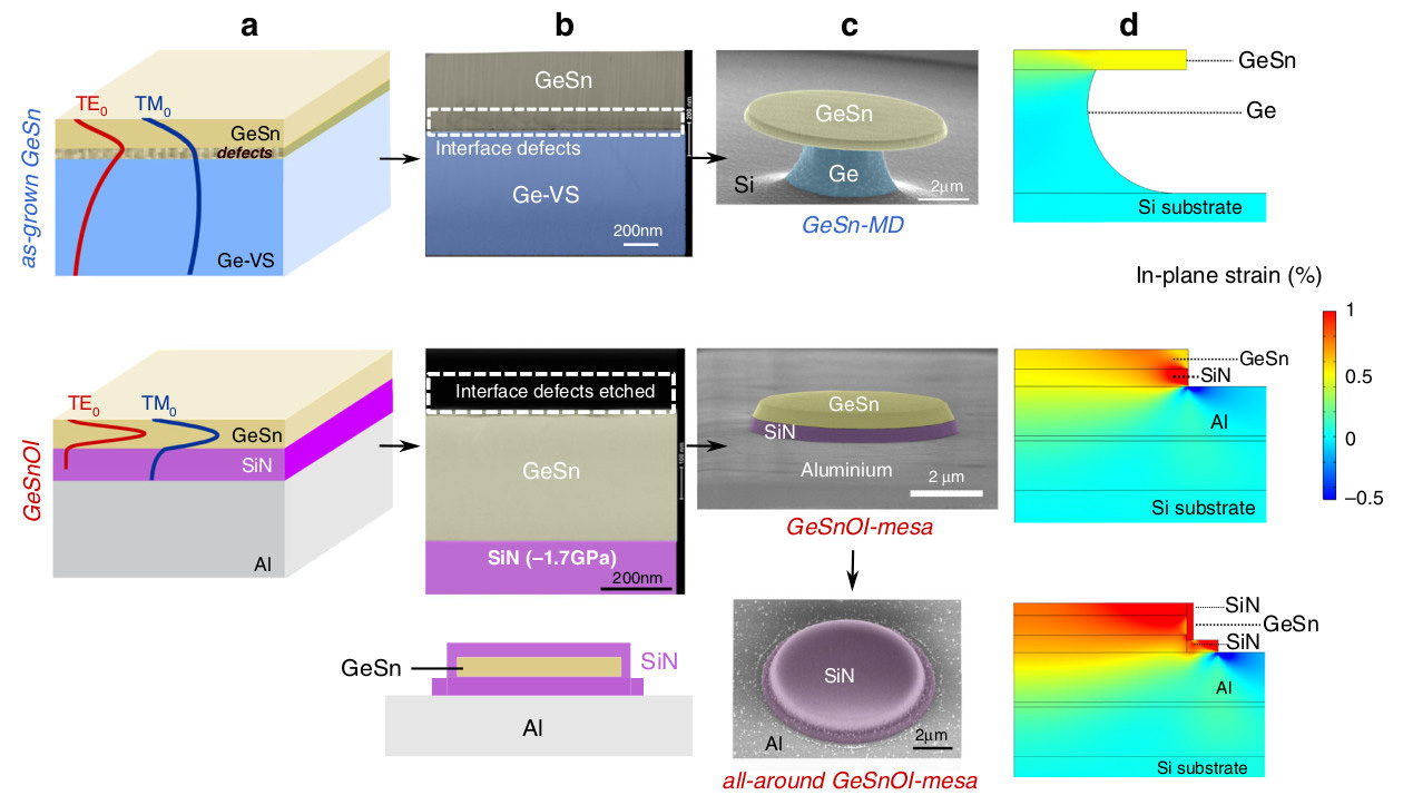
Figure 1: a Schematics of as-grown GeSn on Ge SRB and GeSnOI stacks together with TE and TM mode profiles of a confined optical wave at a 2.4μm wavelength. b Transmission electron microscope images of as-grown GeSn on Ge SRB and of GeSnOI stacks. c Scanning electron microscopy (SEM) images of GeSn and GeSnOI and all-around strained microdisk cavities. (d) In-plane strain variation, analyzed by finite-element modeling (FEM), of GeSn and GeSnOI microdisks.
The mushroom microdisks use the refractive index contrast with air to give 95% confinement of the transverse electric (TE) mode and 78% for the transverse magnetic (TM) mode of the whispering-gallery mode excitations of the circular structure.
The microdisk on SiN/Al obtained through wafer bonding gave a GeSn-on-insulator (GeSnOI) profile. The aluminium provided thermal management through its heatsink properties. The optical confinement was provided by the SiN. The growth Ge/Si substrate was removed by selective etching. Further etching removed the defects that arose at the GeSn/Ge interface during growth. The defect removal and further thinning resulted in a 400nm GeSn layer. The optical confinements for TE and TM modes were 93% and 77%, respectively.
The GeSn on SiN was slightly tensile strained, which could be enhanced and made more homogeneous throughout the layer by adding a top SiN layer. Raman spectroscopy suggested that the injected equivalent biaxial tensile strain in the structure with SiN top stressor was 0.55%, compared with 0.1% without the added layer.
The researchers comment: “The SiN stressor thus enabled us to modify the strain state of our GeSn 10.5% alloy, from a −0.5% compressive state to a 0.55% tensile state, e.g. a shift by ~ +1% of the strain. Band-structure engineering was thus feasible without changing the Sn content.”
Devices with a 7μm-diameter mushroom or mesa microdisk were subjected to pulsed optical pumping of 1550nm wavelength at 77K. The threshold for the mushroom lasing was 45kW/cm2. This was more than halved to 20kW/cm2 for the GeSnOI structures. The GeSnOI mesa output intensity was around 60x that for the mushroom microdisk above laser threshold, and around 4x below.
A number of factors led the team to believe that the GeSnOI mesa absorbed less of the pump beam than the mushroom MD. The researchers comment: “We can thus assume that the improved PL [photoluminescence] signal below the threshold, despite the given above consideration, goes to the sense that carrier losses from non-radiative recombination process are partly reduced with the GeSnOI mesa, which could also partly explain such dynamic gain and threshold improvements.” They believe that improvements in design, such as increasing the SiN layer thickness, could enhance absorption of the pump beam.
Increasing the temperature resulted in the laser action stopping at 80K for the mushroom microdisk, but at 135K for the GeSnOI mesa structure. The characteristic temperature for the threshold increase of the GeSnOI mesa was 40K.
Varying the GeSnOI mesa diameter gave a range of thresholds at 75K of 20-45kW/cm2 for the respective diameters of 3-9μm. The mushroom microdisks only lased with diameters above 6μm with thresholds in the range 35-75kW/cm2 up to 9μm diameter. While the maximum lasing temperature increased to 80K for the larger diameter mushroom microdisks, the GeSnOI mesa had reduced lasing 140-120K in the diameter range 3-9μm. The higher lasing temperatures for GeSnOI mesas was attribute to higher crystal quality.
The team was disappointed in its expectations of improved performance from adding the SiN stressor on top. The threshold for a 3μm-diameter disk was 15.5kW/cm2, compared with 12kW/cm2 for the disk without stressor. Also, the maximum operating temperature was 130K rather than the 140K achieved without the stressor layer.
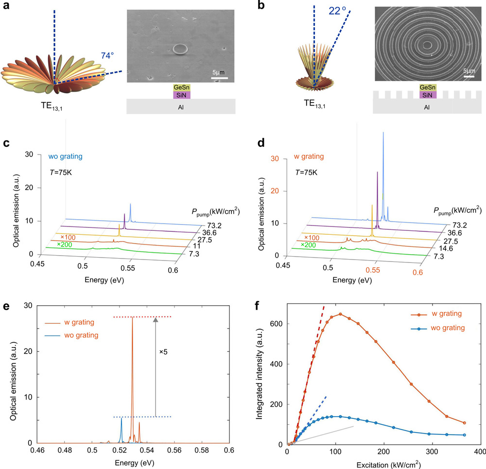
Figure 2: a, b SEM images and calculated emission patterns of 4μm-diameter GeSnOI mesas without and with Al circular grating (7 rings spaced by 3μm with a duty cycle of 50%). c, d Power-dependent spectra without and with Al circular grating. e Spectra with and without grating for 73.2kW/cm2 excitation density. f Light-light power curves of GeSnOI lasers with and without grating.
The researchers also improved the vertical light extraction by placing a GeSnOI mesa laser within a circular grating cut into the Al heatsink layer (Figure 2). Normally light extraction from microdisk lasers is complicated by the radiation pattern being at a large angle to the vertical. Often light collected in microscope objectives is from out-of-plane leakage rather than from the laser radiation mode. Such leakage is unwanted from the perspective of reducing laser thresholds.
The GeSnOI mesa laser with grating was expected to redirect some 30% of the total flux into x50 objective with 0.65 numerical aperture. By contrast, the expectation without a grating was of the order 2.4x10⁻⁵. In practice, the enhancement was around 5x above laser threshold, corresponding to a maximum collected peak power of 20–30μW. Below threshold the collected spontaneous radiation was similar with and without grating.
https://doi.org/10.1038/s41377-021-00675-7
The author Mike Cooke is a freelance technology journalist who has worked in the semiconductor and advanced technology sectors since 1997.


