


News: Optoelectronics
21 January 2021
KAUST contributes to development of perovskite-based MQWs for opto devices
Providing expertise for technologies in electron microscopy, secondary-ion mass spectrometry (SIMS), nuclear magnetic resonance (NMR), surface characterization and optical microscopy, members of the Surface Science Lab at Saudi Arabia’s King Abdullah University of Science and Technology (KAUST) Imaging and Characterization Core Lab (IAC) have collaborated with the research teams of KAUST professors Osman Bakr, Omar Mohammed and Boon Ooi and scientists in South Korea on a project to develop a new approach for fabricating a perovskite-based artificial multiple quantum well (MQW) architecture.
The new semiconductor MQW structure can be used for manufacturing cheaper, high-performance optoelectronic devices (Kwang Jae Lee et al, ‘Perovskite-Based Artificial Multiple Quantum Wells’, Nano Lett. 2019, 19, 6, 3535–3542). IAC’s Surface Science Lab team members utilized their expertise to characterize and confirm the proposed architecture of the new device.
Advances in perovskite semiconductors
Since the nanoscale engineering of silicon through deposition processes to control its properties — for example, to produce solar cells — is time consuming and expensive, scientists have searched for alternative semiconductor materials. Perovskites comprise an emerging family of semiconductors that are low-cost, promising and efficient energy materials used in optoelectronics and photonic devices in place of silicon. Unlike silicon, the optical and electronic behaviors of perovskites can be easily tuned using different compositions and simple deposition techniques.
The materials have the same crystallographic structure as calcium titanium oxide, the first perovskite crystal discovered, and perovskite compounds generally have the chemical formula ABX3.
“[Perovskites’] tremendous variety of structures, phases and dimensionalities makes [them] an excellent candidate for a broad array of applications, such as solar cells, photodetectors, light-emitting diodes (LEDs), and x-ray imaging (scintillators),” the researchers say.
Building quantum wells
As heterostructures comprising a thin layer of one type of semiconductor between two layers of another type of semiconductor with a different energy gap (so that electrons in the middle layer have a lower energy than electrons in the outer layers), quantum wells constrain electrons in the middle layer, limiting motion to two dimensions. The well material’s properties are also altered, and the effect can be increased by combining several quantum wells into a single stack, creating MQWs.
“MQWs have technologically revolutionized traditional LEDs, laser diodes, optical modulators, and switching sensors,” says the research team. “They have also facilitated conceptually new iterations of device applications… and have led to groundbreaking studies of peculiar quantum phenomena.”
To construct MQW stacks, scientists often use epitaxial methods (depositing crystalline film onto a crystalline substrate) with gallium arsenide or gallium nitride involving expensive processes. However, the KAUST research team reckoned that a different method was needed to use the MQW structure in perovskite devices.
“Existing MQWs have been mostly restricted to conventional semiconductor materials,” the researchers note. “[These materials] demand time-consuming and capital-intensive processes such as metal-organic chemical vapor deposition (MOCVD) and molecular-beam epitaxy (MBE)… The requirements have inhibited the scope of MQWs to niche and high-end applications and prevented them from becoming a ubiquitous part of energy, lighting and sensing applications,” they add. “Perovskites offer immense potential for realizing MQWs that could overcome the limitations of conventionally fabricated semiconductor heterostructures.”
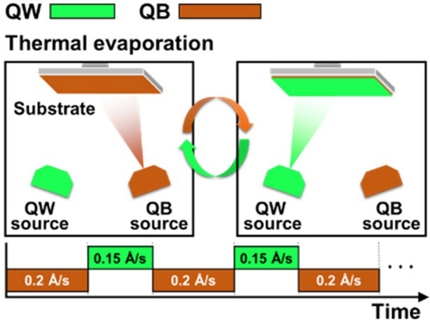
The research team created the artificial MQWs using the simple laboratory technique of thermal evaporation. Using powder of CsPbBr3 for the chosen perovskite well material and the barrier material TPBi (2,2 ,2(1,3,5-benzenetriyl)tris-(1-phenyl-1Hbenzimidazole)), the team found that the powders evaporated when heated in a vacuum chamber. The vapor particles then traveled to the glass substrate, where they formed a film. Alternating between heating the TPBi and the CsPbBr3 created the quantum wells.
An improved method
“Compared to the standard epitaxial methods for growing semiconductor films, the new method is cheaper since it can be performed using a simple thermal evaporator, an instrument available in most research labs,” note the KAUST researchers from Bakr and Mohammed’s teams. “The evaporation method can also be used with any substrate. Moreover, the new approach leads to improved optical properties and energy conversion efficiency,” they add.
“The first major step was to create and to characterize successfully a sample made of two semiconductor materials stacked in form of multilayers, where each layer should have a well-defined thickness,” explains Nimer Wehbe, IAC staff scientist, surface science, who took part in the work.
The sample fabrication step — upon which the success of the developed approach was based — was characterized and studied by Wehbe and Mohamed Nejib Hedhili, IAC team lead, surface science. By employing the resources available in IAC’s Surface Science Lab, they assisted the researchers with analyzing the MQW structure.
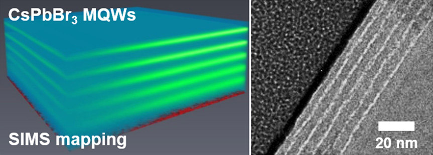
“Using a secondary-ion mass spectrometry technique (SIMS), we were able to provide an elemental 3D mapping confirming that the required architecture of perovskite-based artificial MQWs was successful,” Wehbe says.
“Through the use of an x-ray photoelectron spectroscopy (XPS) technique combined with Kraut’s method, we were able to determine the type of band alignment between the barrier material (TPBi) and the well material (CsPbBr3 perovskite). A type-I band alignment between CsPbBr3 and TPBi was obtained, allowing for a high-performance optoelectronic device,” states Hedhili.
“The new perovskite-based artificial MQWs pave the way toward widely available semiconductor heterostructures for light-conversion applications that are not restricted by periodicity or a narrow set of dimensions,” the research team notes in their paper.
“Our IAC staff scientists are working very hard to provide the KAUST research community with first-class technical expertise to match the cutting-edge instrumentation in the lab,” says Kun Li, acting facilities director overseeing IAC. “In the research work published in Nano Letters, our scientists not only provided the 3D elemental distribution information to confirm the quantum well structure, but they also shed light on its band alignment, which would not have been possible without solid theoretical background in the field.”


