


News: Optoelectronics
28 January 2021
On-chip III-N LED/photodetector integration
Researchers in China have been studying the on-chip integration of indium gallium nitride (InGaN) light-emitting diodes (LEDs) and photodetectors (PDs) [Jing Li et al, Journal of Lightwave Technology, published online 5 January 2021].
The team from Southern University of Science and Technology, Huazhong University of Science and Technology, Shenzhen University, and Guangdong Deli Opto Co Ltd found that centrally placed photodetectors were optimal in terms of response and light-emission uniformity.
Co-integration of LEDs and photodetectors could be useful for real-time monitoring of light output in many lighting applications. Previous attempts at such on-chip integration have used devices placed at some distance from each other, of the order tens or hundreds of microns apart.
The device material used by Li et al was 6μm InGaN/GaN with an active region consisting of multiple quantum wells (MQWs), grown on 4-inch sapphire by metal-organic chemical vapor deposition (MOCVD). The material was fabricated into four types of 1000μmx1000μm LED, incorporating electrically isolated 280μmx280μm photodetector regions in different positions (Figure 1). The gap between LED and photodetector was 10μm.
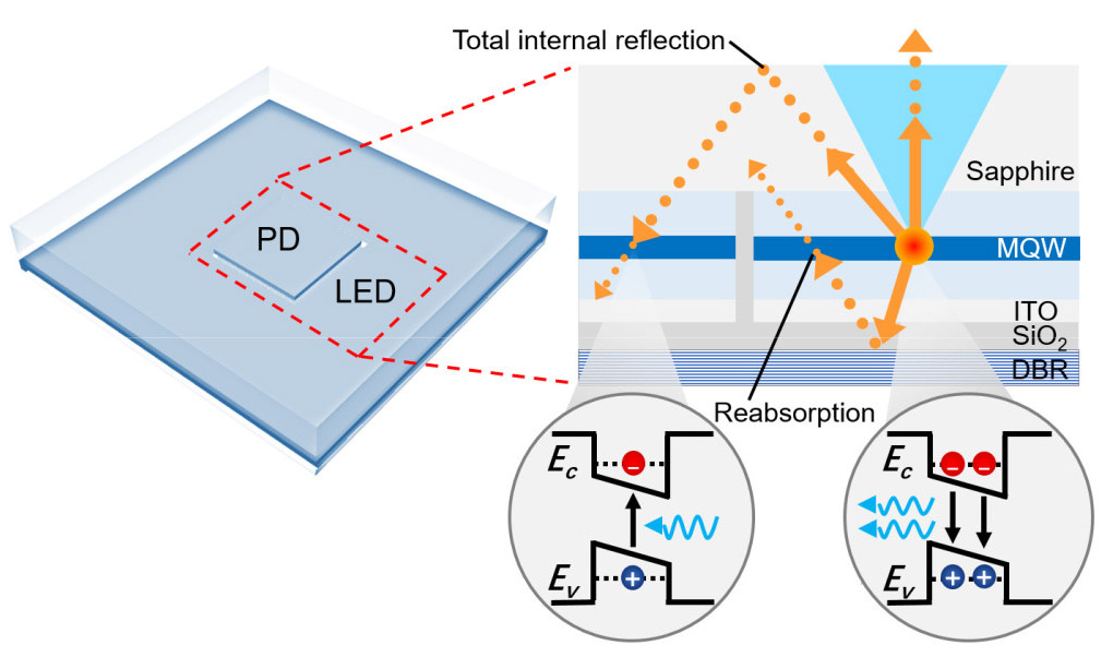
Figure 1: Working principle of LED-PD device.
Fabrication involved inductively coupled plasma (ICP) etching to the n-contact layer, indium tin oxide (ITO) current-spreading layer deposition, mesa isolation etch to the sapphire substrate, metal electrode deposition, silicon dioxide (SiO2) passivation, 23-pair silicon/titanium dioxide dielectric distributed Bragg reflector (DBR) deposition, metal pad deposition, rapid thermal annealing (RTA), substrate thinning, and dicing into separate chips. The chips were flipped onto printed-circuit boards for testing.
The LED output power reached 103.5-106.6mW at 100mA current injection, increasing linearly over the 0-100mA range. The forward voltage at 20mA was 2.73-2.75V. With increasing current in the range 10-100mA, the peak wavelength shortened from 443nm down to 441nm, while the spectral width increased from less than 18nm to more than 20nm. The response peak of the photodetector section was less than 410nm, but the peak was broad enough for there to be some response to the LED.
The researchers comment: “With the increase of wavelength, the response curve exhibits a gradually reducing trend rather than a sharp decline, which is mainly due to the band-tailing effects caused by a combination of the QCSE [quantum-confined Stark effect] and indium content fluctuations in the InGaN/GaN MQWs. The responsivity can be extended to ∼442nm, which overlaps the emission spectrum by ~30nm.”
The photodetector section showed little response to ambient light, showing a current-voltage behavior almost identical to dark conditions (Figure 2). The researchers explain this partly by pointing to the InGaN/GaN LED material being optimized for LED fabrication and not for broadband visible light detection. There are also differences between the ability to couple in external light, compared with the strong total internal reflection of the LED-generated light from the GaN/sapphire refractive index contrast.
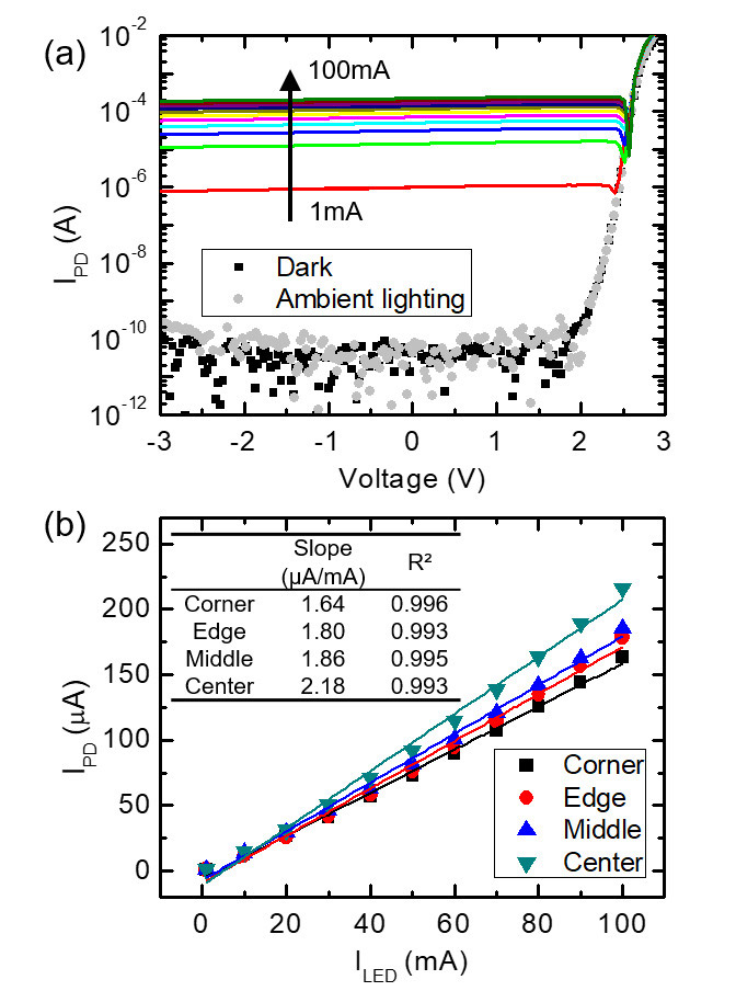
Figure 2: (a) Photodetector current (IPD) versus voltage with varying LED current injection. (b) IPD versus LED current (ILED). Solid lines represent fits to scattered data points. Inset summarizes slope and R2 correlation of fitting lines.
The position of the photodetector was significant for detecting light from the LED with centrally placed photodetectors having 33% greater photocurrent response than corner ones at 100mA injection. The central position was also best for ensuring LED emission uniformity.
The researchers also applied yellow phosphor to the sapphire emission side of the device to get ‘white’ light with (0.32,0.33) CIE color coordinates. The response of the on-chip photodetector compared with a silicon-based photodetector at 3mm above the LED was 1.41x at high current injection, and 1.25x at lower current injection. The researchers point out that at high current the peak LED wavelength is shorter, and shifted towards that of the photodetector response, giving greater spectral overlap and hence photocurrent.
LED/photodetector integration LEDs Photodetectors InGaN/GaN GaN MOCVD
https://doi.org/10.1109/JLT.2020.3048986
The author Mike Cooke is a freelance technology journalist who has worked in the semiconductor and advanced technology sectors since 1997.


