


News: Microelectronics
2 July 2021
Boron arsenide thermal management
University of California Los Angeles (UCLA) and Irvine Materials Research Institute in the USA are proposing the use of boron arsenide (BAs) as a thermal substrate for power electronics devices such as gallium nitride (GaN) channel high electron-mobility transistors (HEMTs) [Joon Sang Kang et al, Nature Electronics, vol4, p416, 2021].
As power densities of electronics systems increase, the need to dissipate waste heat becomes more critical to avoid thermal failure. This needs a combination of high-thermal-conductivity materials and the ability for heat to cross material boundaries.
The GaN material/devices and BAs were bonded using thin aluminium oxide (Al2O3) layers on both materials, applied using 10-cycle atomic layer deposition (ALD) at 473K. The surfaces were exposed to oxygen plasma before bonding to activate the interfaces. After bonding, the assemblies were annealed at 773K in vacuum.
The thermal stability of the process was confirmed by cycling the samples between room temperature and 600K, and the relevant properties measured. The researchers state: “All the samples were measured with consistent results and no appreciable degradation.”
The HEMT devices were produced on silicon. The device layers were 1μm GaN channel/buffer and 20nm AlGaN barrier grown on ~1μm AlGaN transition material to the silicon lattice. The 100μm-width HEMTs were two-finger devices at 34μm gate pitch. The devices were prepared for bonding to BAs with selective wet etching away of the silicon substrate and AlGaN transition layers.
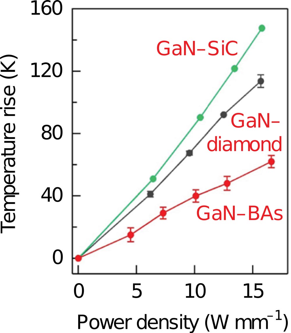
Figure 1: GaN temperature as function of power density, measured using Raman spectroscopy on drain side at lateral distance of 0.5micron from the T-gate edge, for GaN transistors on BAs, diamond and SiC.
The HEMT on BAs showed improved thermal performance over similar devices on silicon carbide or diamond (Figure 1). At a power density ~15W/mm, the GaN-BAs HEMT suffered a hot-spot temperature rise of 60K, much lower than the 110K for GaN-diamond and 140K for GaN-SiC.
The researchers attribute the improved performance of BAs to a combination of high thermal conductivity and low thermal boundary resistance (TBR), relative to the other materials. In fact, the thermal conductivity of BAs is ~1300W/m-K, while diamond’s is ~2200W/m-K. The value for SiC is ~400W/m-K. The thermal boundary conductance (reciprocal of TBR) of GaN/BAs was measured using time-domain thermoreflectance, giving a value of ~250MW/m2-K (about eight times higher than that of GaN/diamond). The researchers estimate that around 35% of the thermal resistance can be attributed to the oxide bonding layers.
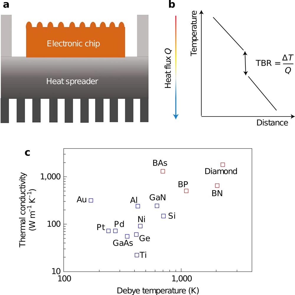
Figure 2: a, Schematic illustrating heat dissipation and thermal boundary resistance (TBR) at interfaces in microchip packaging. b, TBR = ΔT/Q, where ΔT and Q are temperature drop and heat flux across interface, respectively. c, Room-temperature thermal conductivities and Debye temperatures of representative metals, semiconductors and high-thermal-conductivity materials.
The team believes that the lower thermal boundary resistance of GaN/BAs over GaN/diamond can be attributed to a better overlap between the properties of the quantized lattice vibrations (phonons) in GaN/BAs. At a simple level, the Debye temperature, derived from the linear spectrum model for specific heat at low temperature, for BAs is much closer to that of GaN (and other common electronic materials) than diamond (Figure 2). The paper details more complicated theoretical work down to the atomic level, aimed at backing up the team’s belief. In particular, a better overlap of the phonon spectra reduces the tendency for phonons generated in GaN to be reflected back at the boundary with BAs, reducing the TBR.
Boron arsenide GaN HEMTs AlGaN ALD SiC
https://doi.org/10.1038/s41928-021-00595-9
The author Mike Cooke is a freelance technology journalist who has worked in the semiconductor and advanced technology sectors since 1997.


