


News: Optoelectronics
3 June 2021
Dislocations in InAs QD lasers on silicon
Researchers in the USA have improved the performance of indium arsenide (InAs) quantum dot (QD) laser diodes on silicon by incorporating trapping layers (TLs) to inhibit the movement of misfit dislocations (MDs) during operation [Jennifer Selvidge et al, Appl. Phys. Lett., vol118, p192101, 2021].
The team from University of California Santa Barbara (UCSB), Quintessent Inc., Intel Corp and Stanford University in the USA see the work as contributing to understanding and controlling crystal defects, which “continues to be the most impactful avenue toward integrating light sources on photonic integrated circuits and closing the gap with native-substrate lasers.” Producing devices directly on a silicon platform promises to significantly reduce the cost of the optoelectronics technology used in telecoms and other data communication applications.
Although vertical threading dislocations (TDs) have traditionally been seen as show-stoppers for laser diodes, unexpected horizontal misfit dislocations have also been found to impact QD laser performance. The formation mechanism of these misfit dislocations in growth on silicon is described in the paper as possibly “unique”, forming after growth as a result of thermal expansion mismatching between the silicon substrate and overlying aluminium gallium arsenide (AlGaAs) layers. Further, “recombination-enhanced dislocation climb” (REDC) can cause shifts of the misfit dislocation layer, generating point defects that further reduce performance.
The researchers produced material for the lasers that incorporated trapping layers (TLs) matching the lattice structure of the quantum wells (QWs) in which the InAs quantum dots were embedded (Figure 1). The trapping layers in the n-type cladding region were In0.15Al0.85As; those in the p-type cladding, In0.15Ga0.85As. These trapping layers were placed in the n- and p-type cladding at either approximately 80nm or 180nm from the QD region. The choice of the trapping layer material compositions were made to minimally affect the band alignments.
![Figure 1: (a) Schematic No-TL laser structure indicating where trapping layers were inserted in TL80 and TL180 structures. (b) Cross-sectional STEM image of TL180 laser structure along [110] zone axis (left) and tilted into a g = 002 diffraction condition (right). Outset: high-magnification image of dashed region. TD rises through QD layers and forms short MD segment (red arrow) and trapped MD (orange arrow) segment at upper TL. Yellow arrows mark several perpendicular MDs lying along upper trapping layer, appearing as short vertical segments in projection, as indicated in the inset schematic.](21061_ucsb_f1.jpg)
Figure 1: (a) Schematic No-TL laser structure indicating where trapping layers were inserted in TL80 and TL180 structures. (b) Cross-sectional STEM image of TL180 laser structure along [110] zone axis (left) and tilted into a g = 002 diffraction condition (right). Outset: high-magnification image of dashed region. TD rises through QD layers and forms short MD segment (red arrow) and trapped MD (orange arrow) segment at upper TL. Yellow arrows mark several perpendicular MDs lying along upper trapping layer, appearing as short vertical segments in projection, as indicated in the inset schematic.
Laser bars were fabricated with facets coated with silicon dioxide/tantalum pentoxide dielectric layers, targeting 60% and 99% reflectivity of the laser emissions. For testing, the devices were aged for 3000 hours at 60°C under automatic current control at twice the initial threshold current. Some devices were weeded out beforehand if they did not demonstrate low enough threshold current (500A/cm2) or high enough output power (10mW) at 20°C.
The researchers studied devices with and without trapping layers that were most impacted by the aging process in terms of output power under a scanning transmission electron microscope (STEM). Without trapping, misfit dislocations formed in the outer QD layers. With trapping, the amount of misfit dislocations in the QD layer was reduced to about 5%.
The devices with the trapping layers placed at 80nm (TL80) performed best in terms of maintaining output power and threshold current over the aging period (Figure 2). The drop in peak output power was only 11%, compared with 20% for the lasers with trapping layers at 180nm (TL180) and 48% when there are no trapping layers. At the same time, the threshold for the TL80 device only increased 9%, compared with 55% for the laser diode with no trapping layers.
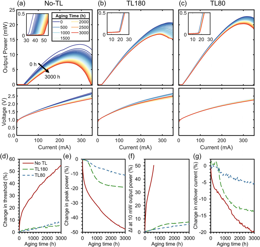
Figure 2: 60°C reliability data from high-performing device of each design. (a)–(c) Light–output and voltage versus current (LIV) measurements at 50h intervals over course of aging for (a) No-TL, (b) TL180, and (c) TL80. (d)–(g) Degradation behavior for same three lasers measured by (d) change in threshold current, (e) change in peak output power, (f) change in current required for 10mW of output power, and (g) change in current at rollover during aging.
The team comments that the performance for devices with trapping layers compares favorably with devices grown on GaAs, and “yields reliability results that are nearly as good as those obtained in threading-dislocation-free lasers grown on native GaAs substrates, despite these trapping layer devices still containing a threading dislocation density (TDD) of 2–4x10⁷/cm2.
STEM analysis suggested that one of the effect of aging was to introduce ‘wavy’/jagged irregularities into the misfit dislocations as a result of recombination-enhanced dislocation climb. “The energy released in this process allows misfit dislocations to increase their length by emitting point defects (i.e. undergo REDC), which explains the sharp degradation in No-TL laser performance,” the researchers write.
Point defects form non-radiative recombination centers, sapping performance and generating heat rather than light. Such heat can lead to thermal runaway, further increasing REDC, and leading to device failure.
The researchers conclude: “As our control over degradation pushes QD laser performance on silicon ever closer to QD lasers on native substrates, we must now look toward implementing this knowledge in advanced integration schemes proposed for photonic integrated circuits. At the same time, it will also be important to revisit other semiconductor materials systems and designs, such as conventional quantum well lasers, where it was once believed that reliable lasers would never be possible in the face of rapid dislocation-based degradation.”
https://doi.org/10.1063/5.0052316
The author Mike Cooke is a freelance technology journalist who has worked in the semiconductor and advanced technology sectors since 1997.


