


News: Optoelectronics
11 March 2021
Monolithic UV LED/photodetector on silicon
Hong Kong University of Science and Technology (HKUST) in China has claimed the first demonstration of monolithically integrated ultraviolet (UV) light-emitting diodes (LEDs) and visible-blind UV photodetectors (PDs) based on the same III-nitride wide-bandgap epitaxial structures grown on silicon [Qifeng Lyu, Huaxing Jiang, and Kei May Lau, Optics Express, vol29, p8358, 2021]
The researchers see opportunities for on-chip optical interconnect and compact opto-isolator applications, along with visible-blind light communication, bio-chemical detection and environment monitoring.
The aluminium gallium nitride (AlGaN) materials were grown on 6-inch (111) Si, using metal-organic chemical vapor deposition (MOCVD). The layer compositions were 5μm GaN buffer, 400nm intrinsic i-GaN, 10nm Al0.2Ga0.8N barrier, and 70nm p-GaN cap. The structure is similar to that used for high-electron-mobility transistors (HEMTs). The HKUST team sees the format as enabling a low dark current measurement in the final photodetectors.
The photodetector was operated in a phototransistor-like way with a 6μmx100μm p-GaN ‘optical gate’ between a pair of ohmic contacts (Figure 1). The 30μmx100μm LED produced photons from the recombination of holes supplied by the p-GaN anode, and electrons from the two-dimensional electron gas (2DEG) that forms near the AlGaN/GaN interface. In HEMTs, and the HKUST photodetector structure, the 2DEG constitutes the channel whose resistance can be controlled by external means (electrostatics, photons, etc).
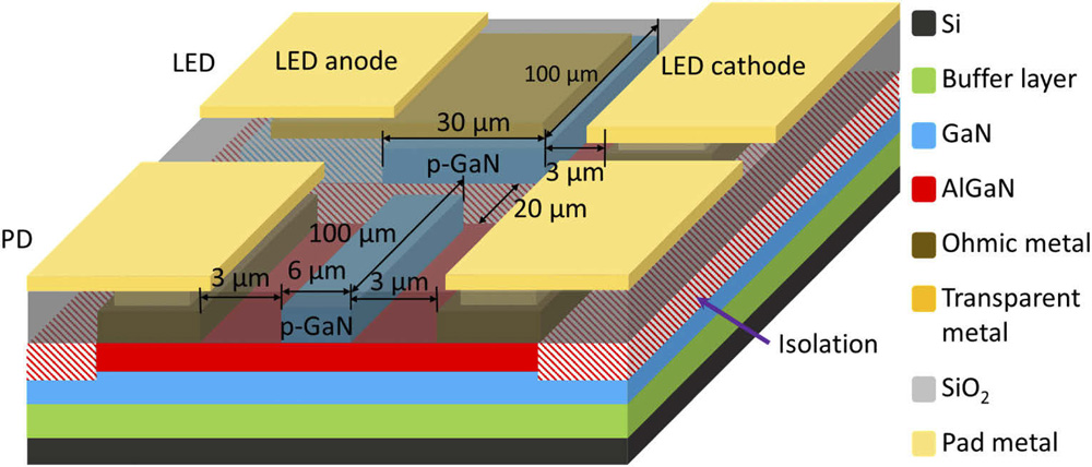
Figure 1: Schematic of monolithically integrated LED and photodetector on p- GaN/AlGaN/GaN/Si platform.
The HKUST team explains: “Mimicking the conventional transistor operation, the current in the channel is controlled by the gate bias through the gate capacitor coupling. In our integrated system, modulation of the current in the ‘channel’ of the photodetector by the spatially separated ‘optical gate’ by the LED is realized by the transmission of UV light in the SiO2, GaN and AlGaN between LED and photodetector.”
The fabrication sequence was: p-GaN patterning for the LED anode and photodetector gate; titanium/aluminium/nickel/gold ohmic contact deposition for the LED cathode and photodetector AlGaN contacts; device isolation with fluorine ion implantation; passivation with 50nm plasma-enhanced chemical vapor deposition (PECVD) silicon dioxide (SiO2); transparent nickel/gold ohmic contact deposition and annealing on the LED p-GaN anode; and, thick nickel/gold contact pad deposition.
Under 5V bias, the photodetector demonstrated a low dark current of 3.9x10⁻⁷mA/mm and a photocurrent of 0.43mA/mm from illumination with 0.024mW/cm2 power UV light ~365nm wavelength from a commercial LED. The researchers describe the photo-to-dark current ratio of 1.1x10⁶ as being “excellent”.
The team adds: “The low dark current is attributed to the depletion of 2DEG at the AlGaN/GaN interface resulting in a high-resistivity channel underneath the p-GaN layer, despite a 5V bias applied.” The UV illumination creates a conductive 2DEG channel under the gate. The “ultrahigh” responsivity of the photodetector was 3.5x10⁵A/W.
The researchers sees these features as enabling the photodetector to achieve “high-sensitivity light detection on signals from the on-chip small-size LED light source even if with a relatively low output power”.
The LED had a high turn-on voltage at ~4.65V, with current injection under forward bias tending to saturate at high biases of ~10V, due to the lateral access regions. The current injected at 10V was 267A/cm2.
The spectral peak of the LED was around 360nm wavelength with a full-width at half maximum (FWHM) of 7nm. The photodetector spectral response cuts off for wavelengths longer than 400nm, raising the prospect of visible-blind applications. [Visible light wavelength range: 380nm-750nm.]
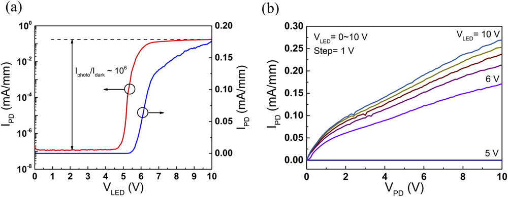
Figure 2: (a) Photocurrent (semi-log and linear scales) of photodetector at 5V bias versus LED bias. (b) PD photocurrent versus voltage drop on photodetector under varying LED bias.
The LED- photodetector combination in a sense operated in a transistor-like way with the LED bias being the gate potential and the photodetector current being the channel (Figure 2). The coupling efficiency (PD/LED current ratio) was 0.022 at 5V photodetector bias, which compares very favorably with 1.1x10⁻⁶ for a reported silicon opto-coupler, ~1x10⁻⁴ for a GaN-based integrated device, and ~4x10⁻³ for an AlGaN-based integrated device.
The ‘frequency response’ of the LED-PD system was tested in a circuit using a Si MOSFET to inject current into the LED. The rise and fall times of the response to a square wave signal were 0.41s and 0.36s, respectively. Since the resistance-capacitance delay of the photodetector was estimated at around 100ns, the main delay factor seems to be a “persistent photoconductivity effect in AlGaN/GaN heterostructure”. The team plans to work on optimizing the p-GaN etch step and the passivation in an effort to eliminate trapping effects, enhancing the response speed. The researchers also suggest that adding a bias to the p-GaN gate of the photodetector could be another avenue to faster response.
https://doi.org/10.1364/OE.418843
The author Mike Cooke is a freelance technology journalist who has worked in the semiconductor and advanced technology sectors since 1997.


