


News: Microelectronics
4 March 2021
HfO2 gate insulator for N-polar GaN
University of Michigan and University of California Santa Barbara (UCSB) in the USA have been studying the potential of hafnium dioxide (HfO2) as a gate dielectric for high-power and high-frequency nitrogen-polar aluminium gallium nitride (AlGaN) transistors, using capacitance-voltage (C-V) measurements [Christopher J Clymore et al, Semicond. Sci. Technol., vol36, p035017, 2021].
The N-polar orientation of AlGaN heterostructure is seen as advantageous in terms of providing a natural back-barrier against current leakage into the substrate, encouraging the confinement of carriers in the two-dimensional electron gas (2DEG) channel. N-polar high-electron-mobility transistors (HEMTs) have achieved superior power-added efficiency (PAE) performance at very high microwave frequencies up to 94GHz over that of Ga-polar devices. Such frequencies are used in radar applications.
To further enable high frequencies and high-power operation, metal-oxide-semiconductor (MOS) gates insulated with high dielectric constant (k) materials such as HfO2 are needed to support reduced gate lengths with good electrostatic control, while avoiding short-channel effects.
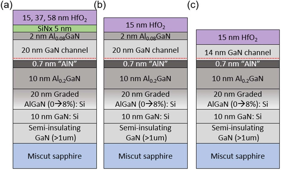
Figure 1: Studied structure schemes: (a) HfO2 on SiN, (b) HfO2 on AlGaN after removal of SiN (MOSCAP-B), and (c) HfO2 on GaN after removal of SiN and AlGaN cap layers (MOSCAP-C.).
The N-polar AlGaN MOS capacitor (MOSCAP) structures were grown on miscut sapphire by metal-organic chemical vapor deposition (MOCVD - see Figure 1). The researchers comment: “A graded Si-doped AlGaN back-barrier is typically used in these heterostructures to suppress current dispersion caused by hole traps at the interface with net negative polarization charge.”
The variations in the studied samples involved the upper layers. A 2nm Al0.08Ga0.92N layer was designed to reduce gate leakage. Silicon nitride (SiNx) dielectric was grown in-situ in the MOCVD chamber as a protection layer in fabrication.
The HfO2 was deposited after electron-beam evaporation and 820°C annealing of ohmic titanium/aluminium/nickel/gold contacts. The HfO2 was applied in a blanket 250°C plasma-enhanced atomic layer deposition (PEALD) process. The gate electrode was titanium/gold.
The capactance-voltage (C-V) behavior was found to be far from ideal at frequencies below 800kHz, which the researchers attributed to slow hole traps. The threshold was also shifted by about 8V, suggesting the presence of negative fixed charges in the dielectric. Annealing at 400°C in argon was found to bring the low-frequency C-V behavior closer to the ‘ideal’. The annealing also reduced high-frequency 1MHz hysteresis from ~3V down to ~1.1V.
A dielectric constant for the annealed HfO2 was extracted using different layer thicknesses – the value was close to that reported elsewhere for the material. Varying the HfO2 thickness was also found to affect the carrier density of the 2DEG that would form the channel in a field-effect transistor. As the dielectric became thicker, the carrier density reduced. The reduction was attributed to the negative charge in the dielectric.
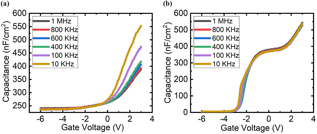
Figure 2: C-V profile measured at different frequencies on (a) MOSCAP-B and (b) MOSCAP-C.
Some samples were studied with the SiNx protection and also the AlGaN top barrier removed, using wet and plasma etching, respectively. The surface damage from the inductively couple chlorine plasma etch was repaired using an ultraviolet ozone treatment, along with a hydrofluoric acid final etch.
Removal of the AlGaN cap was found to be necessary to achieve pinch-off. The team comments: ”These MOSCAPs showed much lower pinch-off voltage which is due to a combination of higher gate capacitance, because of lower distance between gate and the channel, and a thinner GaN channel which leads to lower 2DEG density in the channel.”
The C-V measurements gave a calculated value for the carrier density at 4.9x10¹²/cm2.
The problem with HfO2 deposition on the AlGaN cap was attributed to pinning of the Fermi level, “perhaps due to chemical reaction between oxygen in HfO2 and aluminum in AlGaN and formation of a poor-quality Al2O3 at the interface”.
https://doi.org/10.1088/1361-6641/abe21c
The author Mike Cooke is a freelance technology journalist who has worked in the semiconductor and advanced technology sectors since 1997.


