


News: Suppliers
5 May 2021
Axus improves process performance for single-wafer SiC CMP
Axus Technology of Chandler, AZ, USA – a provider of chemical-mechanical polishing/planarization (CMP), wafer thinning and surface-processing solutions) – has been working to develop and improve CMP process performance and hardware capability for single-wafer silicon carbide (SiC) CMP applications. The primary focus of these efforts include: (1) thin/fragile wafer handling reliability, (2) premium substrate flatness (total thickness variation, or TTV), (3) substrate surface quality, and (4) reduced cost of ownership (CoO).
Based on the architecture of the Capstone CMP system, coupled with the firm’s Crystal carrier specifically designed for fragile wafer handling and advanced profile control, Axus has demonstrated process performance that has so far met or exceeded all customer specifications.
Axus has successfully handled and processed 150mm diameter SiC substrates from SEMI-standard thickness of 350µm down to 175µm, without the need for temporary bonding or handle wafers to support these substrates, as shown in Figure 1.
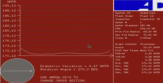
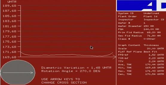
Figure 1. Wafer diameter scan in top image shows a 150mm SiC substrate with average thickness of 171µm pre-CMP. Wafer diameter scan in bottom image shows the same wafer with an average thickness of 170.4µm post-CMP. TTV is reduced during CMP.
As is also shown in Figure 1, in addition to fragile wafer handling capability, Crystal carriers also provide the ability to accurately control the material removal profile during CMP, allowing customers to reduce pre-CMP TTV and produce premium-quality, sub-micron TTV substrates. The market demand for such substrates will continue to drive the high end of SiC wafer pricing and supplier profit margins, says Axus.
In other cases, Axus has demonstrated the ability to reduce substrate TTV by several microns during full CMP processing (Si-face and C-face) during customer process demonstrations.
For surface quality optimization, Axus works closely on both CMP consumables development and process optimization on Capstone. These efforts have resulted in the ability to generate sub-Angstrom (Ra) surface finish with a single-step process (see Figure 2).
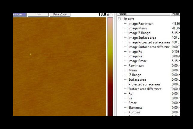
Figure 2. AFM image on Si-face after single-step polish showing 0.8 Angstrom Ra surface finish.
Capstone is said to be the only advanced CMP tool on the market that supports both single-wafer and dual-wafer processing. Dual-wafer processing has been demonstrated to reduce CMP consumables CoO by as much as 50% compared with existing processes of record used on more mature CMP tools.
Since reducing SiC CMP CoO requires faster removal rates and corresponding process throughput, SiC CMP processes typically run at higher wafer pressures and rotation speeds - also known as PV value (pressure x velocity) - compared with other, more mature CMP applications such as silicon. Process temperature becomes a limiting factor as the PV value increases.
Axus has developed a proprietary process cooling system that enables high-PV-value CMP processes that substantially increase the material removal rate without exceeding the maximum temperature limits of other components of the CMP process, particular the polishing pad (see Figure 3).
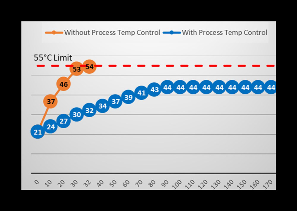
Figure 3. The difference in process temperature with and without process cooling technology developed by Axus (based on pad surface temperature measured by pyrometer), at 5psi wafer pressure.
Process temperature control further enables dual-wafer processing for managing the process temperature in both single-wafer and dual-wafer process scenarios. Based on the Capstone architecture, both platens can perform dual-wafer processing simultaneously, resulting in parallel processing of four wafers concurrently. Capstone is claimed to be the only advanced CMP tool on the market that can process this many wafers in parallel, further improving its throughput advantage.
Recent process improvements have yielded a material removal rate above 10µm per hour on the silicon face. As a breakthrough for single-wafer silicon carbide CMP, Axus is providing SiC wafer suppliers with what is claimed to be the most advanced CMP system on the market and unmatched performance benefits. The Capstone CMP system, coupled with the firm’s Crystal carrier (specifically designed for fragile wafer handling and advanced profile control), delivers premium-quality SiC substrates with sub-micron TTV and sub-Angstrom surface finish. The net result for Capstone users is higher throughput while significantly reducing consumables usage and cost of ownership (CoO).


