


News: Microelectronics
6 May 2021
Fujitsu demonstrates X-band GaN HEMT on AlN
Japan’s Fujitsu Ltd has claimed the first demonstration of output power characteristics for X-band (8-12GHz) gallium nitride (GaN)-channel high-electron-mobility transistors (HEMTs) produced on aluminium nitride (AlN) substrate [Shiro Ozaki et al Appl. Phys. Express, vol14, p041004, 2021].
GaN-based HEMTs have a wide range of potential applications for high-frequency and high-power applications such as radio frequency (RF) power amplifiers in wireless base-stations and radar systems. The technology is particularly attractive in enabling higher output power density, extending communication distances.
The use of an AlN substrate enabled a higher-Al-content AlGaN buffer to be used in conjunction with a thin GaN two-dimensional electron gas (2DEG) channel, compared with structures grown on more conventional silicon carbide (SiC). The 200nm-thick channel was designed to reduce leakage current and improve pinch-off. This high-Al-content AlGaN buffer created an effective back-barrier through charge polarization effects of the different ionicity of the chemical bonds, and large conduction-band offsets, relative to GaN.
The advantage of AlN over SiC in growing AlGaN with higher Al contents and lower dislocation density is due to the closer lattice match with AlN. The effect of lattice mismatch limits AlGaN on SiC to less than 15% Al content before a substantial density of dislocations is generated.
Some research has explored the use of GaN substrates to reduce dislocations, but there would be potential thermal management issues due to a lower thermal conductivity (230W/mK). By contrast, AlN and SiC are much better in this respect, with conductivities of 341W/mK and 420W/mK respectively. Previous reports of HEMT on AlN have focused on high-temperature operation with AlGaN channels, which suffer reduced mobility from alloy scattering.
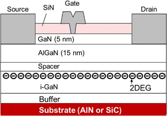
Figure 1: AlGaN/GaN HEMT structure.
The team fabricated HEMTs (Figure 1) with gate length, gate width and gate-to-drain length of 0.25μm, 50μm and 3μm, respectively. A range of comparison devices was produced on SiC substrates (Table 1). The materials were produced using metal-organic vapor phase epitaxy (MOVPE) on AlN or SiC. The 1-inch (0001) AlN substrate was created using physical vapor transport (PVT), resulting in less than 103/cm2 dislocation density and ~1nm root-mean-square surface roughness.
The ohmic source-drain electrodes of the HEMTs were titanium/aluminium, and the gate was nickel/aluminium. The devices were passivated with silicon nitride.
While the maximum drain current for the HEMT on AlN reached more than 1A/mm, the devices on SiC had current all below 1A/mm, and device D had a maximum current as low as 0.7A/mm. Also, the higher-drain-current devices on SiC paid a penalty in terms of breakdown voltage, which was reduced from ~270V for D down to ~160V for F. By contrast, device A on AlN had a breakdown ~250V, close to that of D. The leakage current for HEMT A was of order 1μA/mm at 20V drain bias, compared with almost 10μA/mm for B and 0.1mA/mm for C.
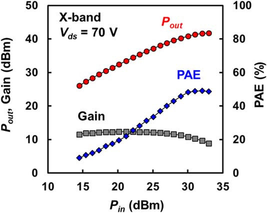
Figure 2: Output (Pout) versus (Pin) characteristics of AlGaN/GaN HEMT on free-standing AlN from X-band load-pull measurements.
Load-pull measurements (Figure 2) for X-band frequencies at 70V drain bias (Vds) achieved peak power-added efficiency (PAE) of 49.1% with associated output power (Pout) of 41.7dBm. The researchers report that these values are equivalent to a power output of 14.7W/mm and 9.6dB gain.
Table 1: Epitaxial structures. Carrier densities determined by Hall measurements. Substrate for A was AlN, the remainder were on SiC. The AlGaN buffer for A had 30% Al, while the remainder on SiC had 5%. A and F included a 2nm AlN spacer.
Sample |
A | B | C | D | E | F |
| GaN channel | 200nm | 200nm | 1000nm | 1000nm | 1000nm | 1000nm |
| AlGaN barrier composition | 31% Al | 31% Al | 31% Al | 17% Al | 17% Al | 17% Al |
| Carrier density (x1013/cm2) | 1.13 | 0.83 | 0.82 | 0.66 | 0.74 | 1.15 |
Saturated output power density reached 15.7W/mm. Reducing the drain bias reduced the power linearly. The team comments: “We believe that the influence of the current collapse because of electron capture was reduced by high 2DEG density of the HEMT on AlN substrate, especially at high Vds.”
Since these results were obtained without source-field plate and optimized dimension enhancements, the researchers believe that even better output power characteristics could be achieved for next-generation high-power RF devices.
GaN HEMT GaN HEMT AlN GaN substrate
https://doi.org/10.35848/1882-0786/abec90
The author Mike Cooke is a freelance technology journalist who has worked in the semiconductor and advanced technology sectors since 1997.


