


News: Microelectronics
21 May 2021
Linear power of graded AlGaN-channel HEMTs
HRL Laboratories and University of Notre Dame in the USA claim a record cut-off frequency-(fT) power density product of 858GHzW/mm for gallium-polar gallium nitride high-electron-mobility transistors (HEMTs) at 30GHz [Jeong-Sun Moon et al, IEEE Electron Device Letters, published online 27 April 2021]. The record was achieved using a graded aluminium gallium nitride (AlGaN) epitaxial material structure and a mini-field plate (FP) T-gate with 60nm gate length.
The potential applications for such devices would be millimeter-order wavelength electromagnetic radio transmission, ‘millimeter waves’ (mmWs), as for proposed 5G and 6G wireless communications.
The epitaxial material structure on silicon carbide (SiC) had a channel structure consisting of graded-composition AlGaN above GaN. The barrier had a 25% Al content. The structure demonstrated a 1423cm2/V-s electron mobility and 9.5x10¹²/cm2 carrier density in the channel.
The fabricated transistors (Figure 1) also featured regrown n+-GaN source-drain contacts in the interest of reducing contact resistance. The source-drain distance was 1.1μm. The mini-FP T-gate had a 50nm overhang on the drain side, designed to reduce gate-to-drain parasitic capacitance effects that reduce high-frequency performance.
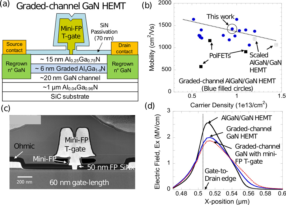
Figure 1: (a) Mini-FP T-gate graded-channel GaN HEMT scheme, (b) measured mobility versus carrier density, (c) scanning electron microscope image of T-gate, and (d) calculated electric field in channel between gate and drain, compared between graded-channel GaN HEMTs and conventional AlGaN/GaN HEMT.
Simulations suggested that the graded channel structure would reduce the peak electric field in the gate-drain gap by 22%. Adopting the mini-FP would reduce this by a further 6%, according to the calculation.
One persistent problem with GaN HEMTs has been current collapse under pulsed and high-frequency operation. The effect in the HRL/Notre Dame device was found to be around 6%, compared with the more than 22% generally reported for T-gate AlGaN HEMTs.
Small-signal frequency performance evaluation between 0.1GHz and 67GHz gave extrinsic cut-off (fT) and maximum oscillation (fMAX) frequencies of 156GHz and 308GHz, respectively. An equivalent circuit analysis suggested that the main factor impacting fT was “gate transit delay associated with the gate-to-source capacitance”.
Continuous-wave passive scalar load-pull power testing on a device with two 37.5μm gate wings from a central stem (2x37.5μm) at 30GHz showed linear power output power density between 2.5W/mm and 5.5W/mm as the drain bias increased between 10V and 20V (Figure 2). Linearity of power output is a key requirement for many wireless communication standards.
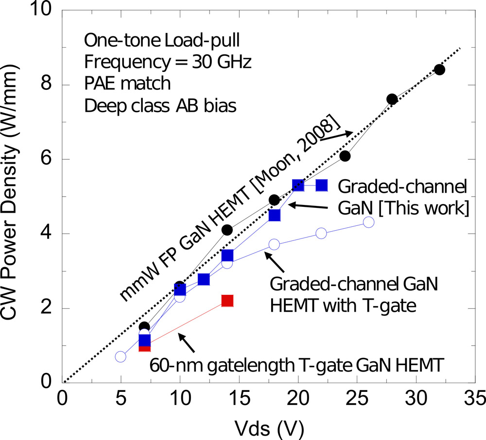
Figure 2: Measured output power density of the graded-channel GaN HEMT versus drain voltage at 30GHz, showing the linear power density scaling.
The associated power-added efficiencies (PAEs) were 70% and 48%, respectively. In these measurements, a fixed load impedance was used, and not optimized as the drain bias increased. The researchers also found that the power density of their transistors was more than 2x that of previous reports of GaN devices with fT ~150GHz.
AlGaN-channel HEMTs AlGaN HEMTs GaN SiC
https://doi.org/10.1109/LED.2021.3075926
The author Mike Cooke is a freelance technology journalist who has worked in the semiconductor and advanced technology sectors since 1997.


