


News: Optoelectronics
13 May 2021
Towards continuous-wave UV-B laser diodes
Researchers in Japan claim the lowest threshold current density so far for a UV-B laser diode (LD) emitting at a wavelength of 300nm [Shunya Tanaka et al, Appl. Phys. Lett., vol118, p163504, 2021]. The 13.3kA/cm2 threshold was achieved by a team from Meijo University, Mie University, Asahi-Kasei Corp and Nagoya University, who focused particularly on optimizing the waveguide thickness and cladding structures.
The researchers see sub-10kA/cm2 thresholds as necessary to realizing continuous-wave operation, which would boost the potential for UV laser diode applications in industry, medicine and biotechnology. A further requirement is for operating voltages to be less than 10V. The UV-B wavelength range is 280-315nm.
In previous work, the team found that one problem with the aluminium gallium nitride (AlGaN) structures of UV-B laser diodes was spontaneous emission from the waveguide layers, which was parasitic on the device performance, reducing charged carrier injection into the laser’s active region. The improved threshold of the latest device structure was obtained by thinning the waveguide to improve injection efficiency and optimizing the cladding to maintain/enhance optical confinement in the laser region.
Inspired by experiment and simulations, the researchers produced an optimized device (Figure 1) on an AlGaN buffer with ~1x10⁹/cm2 dislocation density deposited on a sputtered and annealed AlN template on sapphire, using metal-organic vapor phase epitaxy (MOVPE). The cladding on the n-side was unintentionally doped (u-AlGaN), while the upper cladding layers were doped with magnesium to give p-type conductivity.
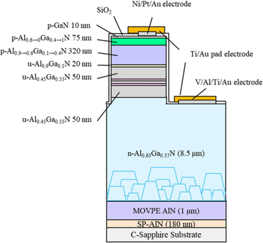
Figure 1: Enhanced UV-B laser diode design on low-dislocation-density AlGaN underlying layer.
The device fabrication process used inductively coupled plasma (ICP) mesa etch and electron-beam evaporation for deposition of the vanadium/gold/titanium/gold n-electrode and nickel/platinum/gold p-electrode. Silicon dioxide was used to electrically isolate the n- and p-electrodes. Contact pads consisted of titanium/gold. Uncoated mirror facets were created using a combination of plasma etch and wet etch in tetramethyl-ammonium hydroxide solution.
A laser diode with 2000μm resonator length and 10μm p-electrode width had a laser threshold current density of 14.2kA/cm2, which compares with 25kA/cm2 for a similar laser diode previously reported by the group. The researchers attribute the improvement to increased injection efficiency and optical confinement.
In experiments on a range of laser diodes with resonator lengths and p-electrode widths, the researchers concluded that there are further factors that need to be investigated with the aim of further reducing threshold currents. The best device with 13.3kA/cm2 threshold featured a 2000μm resonator and 15μm-wide p-electrode (Figure 2).
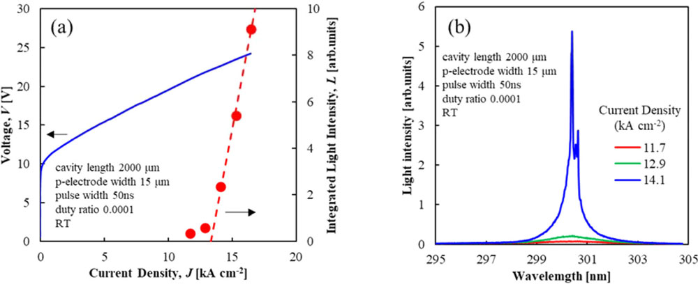
Figure 2: (a) Current density-voltage and -light output characteristics and (b) lasing spectrum of 2000μm resonator laser diode with 15μm-wide p-electrode.
The experimental preparation involved two devices (Figure 3) grown on an underlying AlGaN buffer with a somewhat higher dislocation density of ~3x10⁹/cm2. The group has previously reported material with AlGaN dislocation densities as low as ~7.5x10⁸/cm2, but opted for the somewhat higher value to shorten growth times.
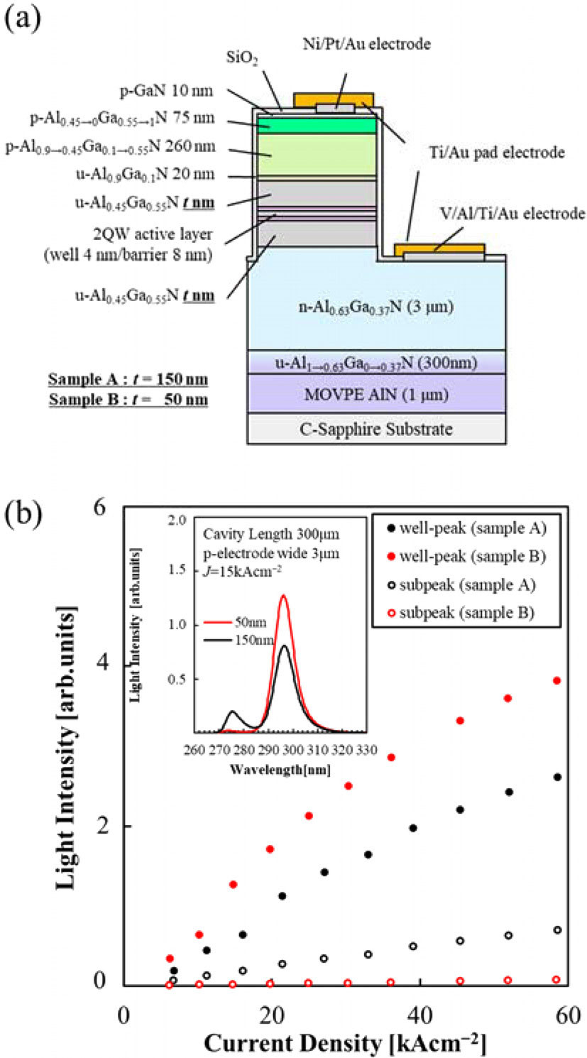
Figure 3: (a) Initial UV-B laser diode design. (b) Current density dependence of well-peak and subpeak emission intensity. Inset: emission spectrum at 15kA/cm2.
The epitaxial design included variable thicknesses of waveguide layers (150nm and 50nm) and upper cladding with two composition-gradient steps to the 10nm p-GaN contact. The thinner 50nm waveguide (sample B) was found to have stronger well peak emission relative to a parasitic subpeak in pulsed operation at room temperature.
The source of the unwanted subpeak is believed to be due to the waveguide layer – experiments on almost identical LED structures without waveguides do not show such emission. Thus, reducing the waveguide thickness might be expected to reduce the subpeak emissions.
Of course, thinning the waveguide reduces optical confinement in the active layer, which is necessary for laser emission, so there is a trade-off. Simulations suggest that the thinner waveguide of sample B allows more light into the absorbing upper cladding layer, reducing laser efficiency. The light absorption was estimated to be 260/cm, relative to 100/cm for the 150nm waveguide structure.
Further simulations were performed to optimize the structure before the 13.3kA/cm2 threshold device was fabricated.
UV-B laser diodes AlGaN AlN template on sapphire MOVPE
https://doi.org/10.1063/5.0046224
The author Mike Cooke is a freelance technology journalist who has worked in the semiconductor and advanced technology sectors since 1997.


