


News: LEDs
22 October 2021
Silicon nanocrystal white LED progress
Fudan University in China reports progress towards effective white light-emitting diodes (WLEDs) based on silicon nanocrystals (SiNCs) [Yu-Chen Zhang et al, Optics Express, v29, p34126, 2021]. The main attraction of such a development is that silicon is about 20,000 times more abundant than gallium, the base material for commercial, efficient III-nitride WLEDs, which are increasingly being deployed to reduce light energy consumption relative to fluorescent and, even more so, incandescent technologies.
Gallium (and its group-III relative indium) are produced as a byproduct of mining for more common materials, such as from bauxite, the source of aluminium, another group-III relative (indium often comes from zinc ores). The average 15 parts per million concentration means purification from such ores is an expensive, painstaking process.
Further attractions of silicon-based light emission is the potentially much easier monolithic integration with low-cost silicon electronics. However, bulk silicon suffers from low efficiency of light emission due to the indirect nature of the bandgap. SiNC structuring can overcome this problem to some extent, creating the potential for silicon-based LEDs. However, while the Fudan research is promising, it seems at the moment that much further development is needed before the technology will become commercial.
The SiNCs were formed using hydrogen silsesquioxane (HSQ with formula [HSiO3/2]n) solution (Figure 1). The solution was dried at 80°C to give a powder, which was then annealed at 1100°C in a 5%:95% hydrogen/nitrogen forming gas mix, creating SiNCs in silicon dioxide (SiO2). This material was ground up in ethanol using a ball mill. The SiNCs were then separated out of the solution using vacuum filtration, etched in a water/ethanol/hydrogen fluoride solution, and stored in pentane. The average SiNC size was ~2.4nm.
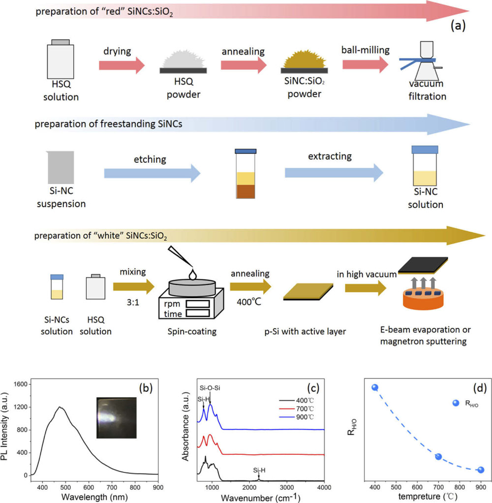
Figure 1: Schematic of freestanding SiNCs and ‘white’ SiNCs:SiO2 thin-film sample process flow (a). PL spectrum of ‘white’ sample, with (inset) photograph of sample under ultraviolet illumination (b). Fourier-transform infrared (FTIR) spectra for ‘white’ samples with different annealing temperature (T) (c). Ratio of adsorbed H to O as function of T (d).
The substrate for the WLED (Figure 2) was <100> p-Si, textured using a water/hydrogen peroxide/hydrogen fluoride solution. Most layers of the device were applied using physical vapor deposition (PVD)/sputtering. The first sputtered layers were 5nm molybdenum oxide (MoO3) hole transfer and 20nm SiO2 rear charge confinement.
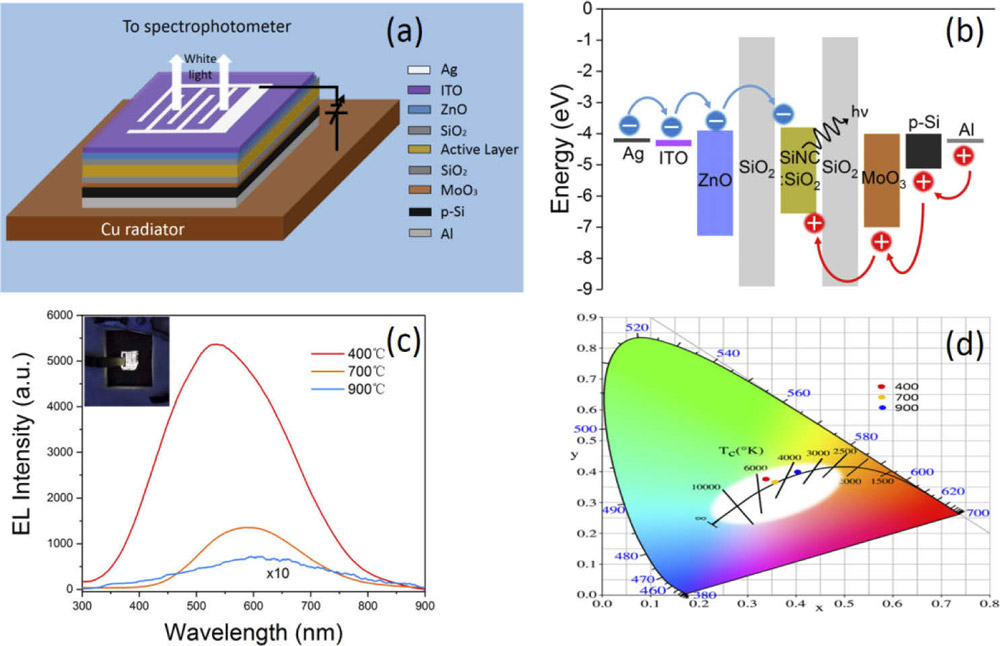
Figure 2: Schematic of SiNC WLED (a). Energy diagrams of components of SiNC WLED (b). EL spectra for different Ts, and inset photograph of Si LWED for 400°C active layer annealing (c). Chromatic chart for SiNC WLEDs for different temperatures (d).
The active layer of SiNCs was applied using spin coating of the crystals in pentane along with HSQ. The structure was annealed at 400°C in nitrogen for an hour. The ‘self-organized’ SiNC source was naturally red-emitting with a peak around 480nm wavelength. The white emission was arranged from forming a colloid of SiNCs and HSQ, and annealing. The photoluminescence quantum yield (PLQY) of the white sample was 11.4%. Varying the annealing temperature gave somewhat different emission electroluminescence spectra of the WLEDs.
The researchers comment: “The white light emission is attributed to the differential passivation of SiNCs, where SiNCs were terminated by both hydrogen (H) and oxygen (O) atoms, with the numbers of adsorbed H and O atoms being different from one SiNC to another.”
The device layers were completed with further sputtering: 15nm SiO2 front charge confinement, 50nm zinc oxide (ZnO) electron transfer, 150nm indium tin oxide (ITO) transparent conductor/current spreader, and 500nm silver (Ag) grid as front electrode. Thermal evaporation of aluminium (Al) onto the back-side of the p-Si substrate gave the rear electrode. The structure was annealed at 400°C in nitrogen to improve the Ohmic behavior of the metal contacts to the device layers.
During testing the WLED was placed on a Peltier cooler and copper heatsink. The peak electroluminescence wavelength was 536nm, 592nm and 613nm, for active layers annealed at 400°C, 700°C and 900°C, respectively. The corresponding color temperatures were 5297K, 4689K and 3686K.
The “best” device was that with the active layer annealed at 400°C. This WLED achieved a peak luminance of 2060cd/m2 at 13.0V bias, while the external quantum efficiency (EQE) was 0.15%. Turn-on came at 3.7V. The peak EQE was 0.16% at 9.8V. By contrast, blue LEDs based on gallium nitride can reach beyond 80% EQE. Commercial WLEDs usually add a yellow or more complex phosphor to spread the wavelengths from blue, reducing the efficiency somewhat.
The emission intensity for a given injection current decayed over time. At 0.52A/cm2 injection, the exponential decay time constant was ~94 hours.
The researchers suggest that practical general lighting based on SiNCs “is attainable by further optimizing the components following the strategy of optimizing the rate of injection and transport of charges, strengthening the confinement of the injected charges within the active layer, increasing the PLQY of the active layer, and enhancing the efficiency of light extraction and the heat dissipation.”
Silicon nanocrystal SiNC White LED ZnO
https://doi.org/10.1364/OE.437737
The author Mike Cooke is a freelance technology journalist who has worked in the semiconductor and advanced technology sectors since 1997.


