


News: Microelectronics
28 October 2021
HVPE p-GaN vertical pn diodes
Japan’s Nagoya University has used gallium nitride (GaN) halide vapor phase epitaxy (HVPE) to produce vertical p+n-junction diodes (PNDs) with “ideal” breakdown voltage [Kazuki Ohnishi et al, Appl. Phys. Lett., v119, p152102, 2021]. Normally, such devices are produced with the slower metal-organic VPE (MOVPE) process. The key to the HVPE p+n-junction diodes was Nagoya’s recent development of an HVPE recipe for p-GaN without detectable silicon contamination.
GaN is being developed to replace silicon in power electronics applications, where high breakdown voltages are needed. The III-nitride material features high critical electric fields, high saturation voltage and high mobility, thanks to its wider bandgap compared with silicon.
MOVPE processes suffer from a tendency for the carbon of the organic precursors to become incorporated in the growing semiconductor material. Carbon is both a deep donor and deep acceptor in GaN. Thus, the presence of carbon reduces the effectiveness of any doping design. To reduce carbon incorporation, MOVPE growth speeds are even further reduced.
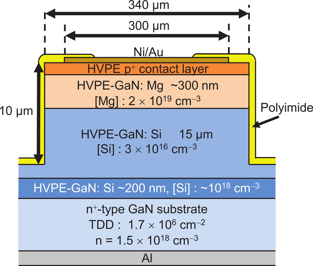
Figure 1: Schematic cross section of vertical GaN p+-n junction diode grown by HVPE. Substrate parameters from supplier.
In vertical power devices, one usually balances thick, lightly doped n-GaN drift layers against thinner, heavily doped p-GaN layers. Thicker drift layers allow higher voltages to be handled by distributing the electric field strength over a longer distance. Such drift layers need low doping to be effective. Carbon impurities impede the achievement of this low n-type doping.
HVPE avoids carbon incorporation by using carbon-free precursors. Here, one needs to control silicon and oxygen impurity incorporation. Unwanted silicon and oxygen can be avoided by using quartz-free equipment.
Until recently, there has been no suitable HVPE process for p-GaN layers. One way around this has been to use hybrid HVPE-MOVPE for the n-GaN and p-GaN layers, respectively. However, diodes produced from such processes suffer from silicon accumulation effects, which lead to high leakage and premature breakdown.
The Nagoya researchers used a freestanding HVPE n+-GaN substrate on which further layers of variously doped GaN were grown by 1050°C HVPE at atmospheric pressure to give the semiconductor material for the diode. The 15μm low-doped n-GaN drift layer was grown at 30μm/hour. The p-type layers were grown at a much slower rate of 3μm/hour.
The Ga precursor was gallium chloride (GaCl) gas from reaction between hydrogen chloride and a Ga melt at 900°C. The nitrogen came from ammonia (NH3). The silicon for n-type doping came from silicon tetrachloride (SiCl4).
The magnesium doping for the p-type layers was sourced from magnesium oxide (MgO). The researchers believe that the MgO reacted with HCl in the system to form MgCl2 before delivery at the growth front. The final heavily doped p-+GaN contact layer was 20nm thick.
The diodes were fabricated into 340μm-diameter inductively coupled plasma etched mesas with nickel/gold (Ni/Au) alloy anode on the p+-GaN contact, and aluminium (Al) cathode on the back-side of the wafer. The Mg doping was activated by 700°C 5-minute annealing after the plasma etch. A 3μm polymide layer was used to passivate the mesa sidewalls.
Secondary-ion mass spectroscopy (SIMS) showed oxygen, carbon and hydrogen concentrations in the 15μm drift layer below the detection limits of 7x10¹⁵, 3x10¹⁵ and 3x10¹⁵/cm3, respectively. In the p-type layer as-grown (i.e. before annealing to drive out the H atoms), the hydrogen concentration increased with Mg doping, passivating the acceptors. The Mg concentration in the drift layer was 5x10¹⁵/cm3, blamed on memory effects (i.e. residual Mg in the reaction chamber from previous p-GaN growth processes).
The minimum ideality factor was 1.6 at 298K, which compares with the range 1.1-2.3 for p+n-junction diodes grown by MOCVD. The breakdown voltage of the device was 874V at 25°C and 974V at 200°C. The increase in breakdown with increased temperature suggests an ideal avalanche multiplication mechanism for the breakdown. “This is because the phonon scattering rate in a semiconductor increases, and it is too difficult to obtain sufficient energy of carriers to cause impact ionization with the increasing temperature,” the team explains.
Further experiments showed a linear increase of the non-destructive avalanche breakdown voltage with temperature. Comparison with theory suggests that the device has “ideal critical electrical field and avalanche capability,” according to the researchers. The breakdown voltage was also found to be in line with that achieved by MOVPE (Figure 2). Reducing the drift layer doping should increase the breakdown voltage.
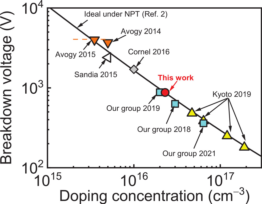
Figure 2: Breakdown voltage as function of drift-layer doping concentration for reported GaN p+n-junction diodes: solid line - ideal breakdown voltage for GaN p+n junction under non-punch-through condition; red circle - latest Nagoya experimental work; other plots - previously reported GaN p+n-junction diodes grown by MOVPE; dashed line - doping concentration range of one group.
The diode did suffer from a higher leakage under reverse bias than similar devices grown by MOVPE. The team says that it is not clear whether this is a specific problem for HVPE growth or not, since the reverse-bias behavior of some MOVPE diodes reported is similar to that of the Nagoya group’s HVPE diodes.
GaN HVPE +n-junction diodes">p+n-junction diodes MOVPE GaN Substrates
https://doi.org/10.1063/5.0066139
The author Mike Cooke is a freelance technology journalist who has worked in the semiconductor and advanced technology sectors since 1997.


