


News: LEDs
27 October 2021
NCSU uses semi-bulk growth of InGaN templates to push emission wavelength into green gap
Researchers at North Carolina State University (NCSU) have developed a new process that makes use of existing industry-standard techniques for making III-nitride semiconductor materials but results in layered materials that can make LEDs and lasers more efficient.
A challenge for making LEDs and lasers has been that there was a limit to the number of holes that you can make in p-type III-nitride semiconductor materials created using metal-organic chemical vapor deposition (MOCVD). “We have developed a process that produces the highest concentration of holes in p-type material in any III-nitride semiconductor made using MOCVD,” claims the paper’s co-author Salah Bedair, a distinguished professor of electrical and computer engineering at NC State. “And this is high-quality material – very few defects – making it suitable for use in a variety of devices.”
In practical terms, this means more of the energy input in LEDs is converted into light. For lasers, it means that less of the energy input will be wasted as heat by reducing the metal contact resistance.
To produce semiconductor materials for use in LEDs or laser diodes, the researchers use semi-bulk growth to produce indium gallium nitride (InGaN) templates, comprising dozens of layers of indium gallium nitride and gallium nitride. These templates were used for the n-type region to reduce complications that arise with the growth of the quantum wells. The insertion of the gallium nitride layer in between the indium gallium nitride layers in semi-bulk reduces defects due to the lattice mismatch between the semi-bulk template and the GaN substrate, as well as filling the pits that form on the surface.
In their new work, the researchers demonstrated that the semi-bulk growth approach can be used for the p-type layer in LEDs to increase the number of holes. This new approach is cost effective from a manufacturing standpoint, since III-nitride-based LED devices can be fabricated in one growth via MOCVD, without a lengthy processing time in between.
Using this technique, the researchers achieved a hole density of 5x1019cm-3 in the p-type material. Previously, the highest hole concentration achieved in p-type III-nitride materials using MOCVD was about an order of magnitude lower.
The researchers also applied these InGaN templates as substrates for LED structures to address the long-running ‘green gap’ problem, where the LED’s output deteriorates when emitting in the green and yellow part of the spectrum.
One of the main reasons for the green gap is the large lattice mismatch between the quantum well light-emitting part of the material when gallium nitride substrates are used. The researchers have demonstrated that replacing the gallium nitride substrates with indium gallium nitride templates results in improved LED performances.
The researchers compared the LED emission spectrum for the same quantum well emitting in blue when grown on GaN substrate and emitting either in green or yellow when grown on different InGaN templates. A 100nm shift in the emission wavelength was achieved due to the application of the InGaN templates.
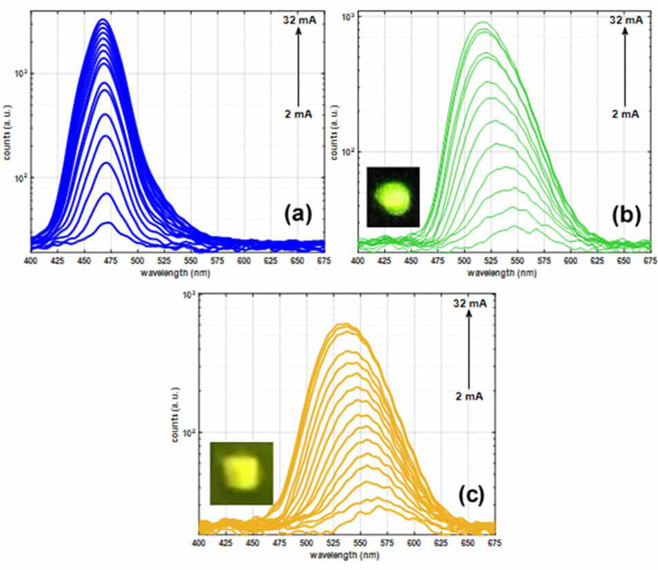
Picture: Electroluminescence measurements of (a) blue LED on GaN, (b) green LED on InGaN template, (c) near-yellow LED on InGaN template. The insets of (b) and (c) show the image of the emission at 1.5mA injection current.
The paper on improved efficiency, ‘P-type InxGa1-xN semibulk templates (0.02 < x 0.16) with room temperature hole concentration of mid-1019cm-3 and device quality surface morphology’, was published on 20 September in Applied Physics Letters (DOI: 10.1063/5.0065194). The first two authors are Evyn Routh and Mostafa Abdelhamid (who are both Ph.D. students at NC State). The paper was co-authored by Peter Colter (a postdoctoral researcher at NC State) and Nadia El-Masry of both the US National Science Foundation (NSF) and NC State).
The paper addressing the green gap in LEDs, ‘Shifting LED emission from blue to the green gap spectral range using In0.12Ga0.88N relaxed templates’, was published on 19 October in Superlattices and Microstructures (DOI: 10.1016/j.spmi.2021.107065). The first two authors are Abdelhamid and Routh. The paper was co-authored by Ahmed Shaker (a visiting scientist at NC State from EinShams University in Egypt).
https://aip.scitation.org/doi/10.1063/5.0065194
www.sciencedirect.com/science/article/abs/pii/S0749603621002639


