


News: Microelectronics
7 October 2021
Ruthenium gate for InP MOSFETs
University of California Santa Barbara (UCSB) in the USA has reported record high transconductance (gm) and subthreshold swing (SS) for planar indium phosphide (InP)-channel metal–oxide–semiconductor (MOS) field-effect transistors (MOSFETs) [Hsin-Ying Tseng et al, Appl. Phys. Lett., v119, p123502, 2021].
The UCSB team used ruthenium (Ru) as the gate metal, applied using atomic layer deposition (ALD). A key aspect was the use of titanium nitride (TiN) as a nucleation/stiction layer on the high-k dielectric part of the high-k metal gate (HKMG) stack. Without the TiN layer, Ru tends to grow in a rough and non-uniform manner. In MOS capacitors, the use of TiN to nucleate Ru was found to reduce frequency dispersion in capacitance-voltage measurements, “suggesting a metal–semiconductor interface with low defect density”.
The researchers suggest that the development of high-performance InP high-electron-mobility transistors could be used in “mm-wave receivers, and in the gate structure of tunnel FETs for ultralow-voltage VLSI logic”.
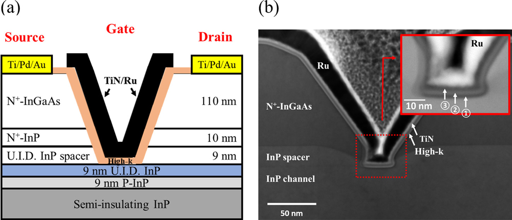
Figure 1: (a) Planar MOSFET schematic cross-section and (b) scanning transmission electron microscope (STEM) image of MOSFET with 30nm TiN/Ru gate. Inset: high-angle annular dark-field STEM image of InP channel. Layers 1, 2, and 3 represent ~1nm AlOxNy, ~2.5nm ZrO2, and ~2nm TiN, respectively.
The researchers deployed the gate stack on planar (Figure 1) and vertical (Figure 2) MOSFETs on semi-insulating iron-doped InP substrates. The epitaxial layers were applied using metal-organic chemical vapor deposition (MOCVD).
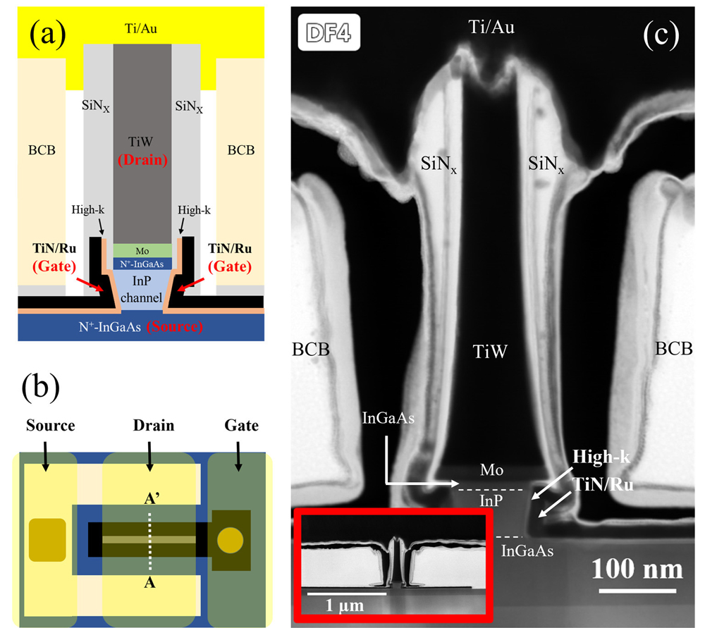
Figure 2: (a) Cross-sectional and (b) top-view vertical MOSFET structure, and (c) cross-sectional STEM image cutting along A and A’, as indicated in (b). P-InP channel length is 50nm, Inset in (c) is large-field image.
The epitaxy for the planar MOSFET began with 9nm zinc-doped p-InP, which compensated for donor impurities of the substrate surface. This was followed by 9nm unintentionally-doped (UID) InP.
The MOCVD was then interrupted to enable the formation of a dummy gate structure, consisting of hydrogen silsesquioxane (HSQ) resist, around which self-aligned source-drain layers would be regrown by MOCVD.
After the MOCVD regrowth, the device structures were electrically isolated using wet etching. The dummy gate was then removed and the surfaces treated to remove oxides. The gate stack was applied using 300°C ALD.
The high-k dielectric part of the HKMG consisted of ~1nm aluminium oxynitride (AlOxNy), ~2.5nm zirconium dioxide (ZrO2). This was followed by ~2nm titanium nitride (TiN) and the ~30nm ruthenium (Ru) gate electrode.
The chemicals used to form the AlOxNy were trimethyl-Al alternated with nitrogen plasma. For the ZrO2, water (H2O) and tetrakis(ethylmethylamido)zirconium (TEMAZ) were used. The TiN came from cycles of tetrakis(dimethylamido)titanium (TDMAT) and nitrogen/hydrogen plasma. The Ru resulted from alternate (ethylbenzene)(1,3-cyclohexadiene)ruthenium (EBCHDRu from Hansol Chemical) and oxygen.
The structure was annealed in hydrogen for 30 minutes to “recover plasma damage at the high-k/InP interface”. The devices were completed with titanium/palladium/gold source/drain electrodes on the heavily n-type indium gallium arsenide (n+-InGaAs) contact layer, and ALD aluminium oxide passivation.
The vertical MOSFET used a semi-insulating InP substrate with MOCVD layers of 90nm n+-InGaAs source, 50nm p-InP channel, and 5nm/10nm n+-InP/n+-InGaAs drain/contact.
Device fabrication began with electron-beam deposition/DC sputtering of the 20nm/500nm molybdenum/titanium-tungsten (Mo/TiW) drain metals, which was then patterned and plasma etched, creating a fin structure. The sidewalls of the fin were coated with 20nm plasma-enhanced chemical vapor deposition (PECVD) silicon nitride (SiNx).
Wet etching cut into the InGaAs drain layer, which was also coated with 20nm Si3N4. Further wet etching into the InP layers (drain and channel) formed the vertical channel. Digital etching based on hydrochloric acid removed native oxides before high-k deposition in an ALD process, as before.
The TiN layer was also made identically, but the Ru metal gate electrode had to be deposited at 250°C, rather than 300°C. Deposition at the higher temperature tended to suffer from precursor decomposition in the more tricky geometry. The lower temperature ran the risk of oxide formation, stunting growth. To stop this, the researchers added hydrogen as a co-reactant in the ALD recipe.
The complete HKMG was annealed as for the planar device. The source contact was Ti/Pd/Au. Ti/Au metal posts were applied to the source and gate contacts. Passivation consisted of 30nm PECVD SiNx. The structure was planarized with spin-on dielectric benzocyclobutene (BCB), which was baked and ashed back.
The device was finished with wet etching to remove the SiNx and excess Ru around the drain electrode, creating a 60nm PECVD SiNx sidewall spacer, and forming the backend wiring/contact pads with Ti/Au.
The Ru/TiN planar MOSFETs were found to have an optimum gate length (Lg) of 80nm in terms of peak gm. Below 80nm, the device suffered from short-channel effects, due to the relatively thick ~18nm channel layers. At 80nm, the peak gm was ~0.75mS/μm, for 0.6V drain bias, claimed as the highest yet reported for InP-channel MOSFETs (Figure 3).
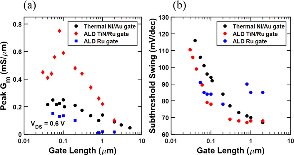
Figure 3: Comparisons of peak gm versus Lg (a) and minimum SS versus Lg (b) for InP planar MOSFETs with thermally evaporated Ni/Au gates, ALD TiN/Ru gates, and ALD Ru gates.
When Lg exceeds 800nm, the Ru/TiN MOSFET also demonstrated “record” low subthreshold swing values of 68mV/decade at 0.1V drain bias. The previous record was 70mV/decade for an InP MOSFET with nickel/gold (Ni/Au) gate metal.
The vertical MOSFET suffered from short-channel effects due to the low aspect ratio of Lg and fin width (50nm:90nm). Also, the channel doping was not sufficient to cut off leakage currents in the off-state. “To overcome this issue, a higher P-channel doping or a higher aspect ratio between Lg and body thickness (tbody) is needed,” the team comments. The peak gm with 0.6V drain reached a respectable 0.42mS/μm. This is close to the value achieved in the 50nm Lg planar device.
https://doi.org/10.1063/5.0058825
www.hansolchemical.com/en/main.do
The author Mike Cooke is a freelance technology journalist who has worked in the semiconductor and advanced technology sectors since 1997.


