


News: Optoelectronics
29 September 2021
Direct-epi InP QD micro-disk lasers on silicon
Hong Kong University of Science and Technology (HKUST) in China claims the first red micro-disk lasers (MDLs) fabricated using material from direct epitaxy of indium phosphide (InP) quantum dots (QDs) on silicon (Si), with a view to the integration of silicon photonics with red (625-700nm) and near-infrared (NIR, 700-1400nm) lasers [Wei Luo et al, Optics Letters, v46, p4514, 2021].
Silicon photonics is seeing much interest from areas such as optical communication, bio-photonics, and sensing. The red/NIR areas of the spectrum accessible to InP QDs are attractive for displays, underwater communication, and molecular diagnostics.
A range of compact light sources integrated into silicon photonics structures is often needed for such applications. Efficient semiconductor light sources are presently made from the various III-V compounds, which often don’t mix easily with silicon production processes. Direct epitaxy, creating monolithic devices, would be much preferred over the direct wafer bonding techniques that presently dominate commercial production.
One barrier to direct epitaxy is the large numbers of defects that tend to be generated inside the III-V semiconductor structures. QDs are less prone to be affected by defects, presumably due to the carrier recombination processes being more confined in the localized states of the individual dots.
The InP QD structures were grown on gallium arsenide (GaAs)/Si templates using metal-organic chemical vapor deposition (MOCVD). A separate three-step MOCVD process was used to create the GaAs templates on (001) Si to which was added three sets of strained-layer superlattices (SLS) separated by 300nm GaAs spacers to further reduce defect density (Figure 1). The SLS consisted of 10 pairs of 9.5nm/12nm In0.16Ga0.84As/GaAs.
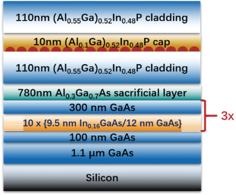
Figure 1: Schematic of InP QD laser structure grown on GaAs/Si template.
The laser structure itself consisted of an aluminium gallium arsenide (AlGaAs) sacrificial layer, AlGaInP lower and upper cladding, and inbetween InP QDs capped with AlGaInP. The QD density was 1.3x10¹⁰/cm2, which compares with 1.2x10¹⁰/cm2 density for QDs grown on bulk GaAs. Close inspection with transmission electron microscopy (TEM) showed the QD dimensions to be of order 40nm diameter and 4nm height. In addition, there was a low density of larger-sized QDs, which created a shoulder on the long-wavelength side of photoluminescence (PL) spectra. QDs on GaAs/Si emitted at somewhat longer wavelengths relative to InP QDs on GaAs. The team attributes the red-shift on GaAs/Si to “residual tensile strain caused by the introduction of SLSs and the thermal mismatch between the III–V material and silicon”.
Fabricated micro-disk lasers measured 1.5μm in diameter. Dispersed silica beads were used as a hard mask for the inductively coupled plasma (ICP) etch process, resulting in columns down to the sacrificial layer. The pedestals were formed using a selective AlGaAs wet etch.
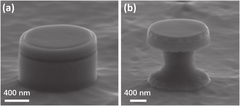
Figure 2: 70°-tilted scanning electron micrograph of micro-disk lasers on GaAs/Si template (a) before and (b) after pedestal formation.
Smooth sidewalls of the circular disk structure (Figure 2) were critical for achieving a ‘whispering gallery’-type mode for the laser cavity. Even well below the lasing threshold, this mode peak was clearly visible in continuous wave spectra from a 514nm pump laser diode at 6.25nW (Figure 3).
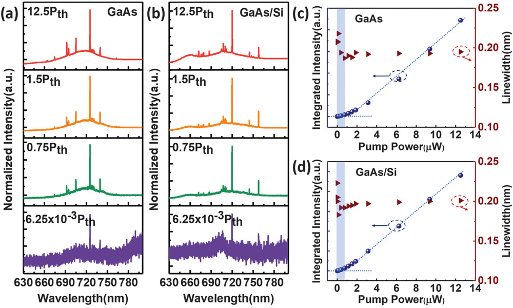
Figure 3: Representative room-temperature power-dependent PL spectra of InP QD MDLs on (a) GaAs substrate and (b) GaAs/Si template, respectively. (c) and (d) Corresponding collected PL intensity and mode linewidth of dominant peak in (a) and (b) as a function of pump power.
The laser threshold pump power was around 1μW for micro-disk lasers both on GaAs/Si and GaAs (Figure 4). The researchers compare this with 30μW threshold reported in 2009 by University of Notre Dame in the USA and Ioffe Physical Technical Institute in Russia for InP QD micro-disk lasers directly bonded onto silicon. In addition, the laser output power increases linearly with the pump power up to 12.5x the threshold value. The lowest threshold achieved was 500nW (0.5μW).
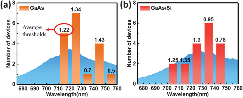
Figure 4: Statistical analysis of lasing behavior of InP QD MDLs on (a) GaAs and (b) GaAs/Si. The numbers on top of each column denote average MDL thresholds. Backgrounds: normalized PL spectra of unprocessed samples.
The researchers conclude: “Direct epitaxy of InP QDs on a high-Al-composition (Al0.55Ga)0.52In0.48P barrier leads to higher QD density, which also contributes to the low threshold of the micro-disk lasers.” The team hopes to fabricate in future electrically pumped micro-disk lasers using similar techniques.
Red micro-disk lasers InP InP quantum dots Silicon photonics MOCVD GaAs templates InGaAs AlGaAs AlGaInP
www.osapublishing.org/ol/abstract.cfm?uri=ol-46-18-4514
The author Mike Cooke is a freelance technology journalist who has worked in the semiconductor and advanced technology sectors since 1997.


