


News: LEDs
2 September 2021
Stacking three III-nitride LEDs
Ohio State University and Sandia National Laboratories in the USA claim the first demonstration of triple-junction cascaded III-nitride light-emitting diodes (LEDs) grown by metal-organic chemical vapor deposition (MOCVD) [Zane Jamal-Eddine et al, Appl. Phys. Express, v14, p092003, 2021].
Stacking LEDs is one way to overcome the limitations in output power density imposed by the effects of efficiency droop at large current density. Tunnel-junction (TJ) structures are used to connect LEDs since they enable electron majority carriers to be transformed to holes for injection into the next stage of the cascade. Producing TJs with a low voltage drop for a given current is a challenge, particularly in an MOCVD growth scheme relative to molecular beam epitaxy (MBE). By contrast, MOCVD is preferred for mass production, and also tends to produce higher-quality active regions.
The epitaxial structures (Figure 1) were grown in one run. Three identical layer sequences were grown on top of each other, consisting of active light-emitting multiple quantum wells (MQWs), followed by a tunnel-junction (TJ) structure, which included a very low-indium-content indium gallium nitride (InGaN) layer, graded from a peak of 6% to 0%. The low content ensured that the layer was transparent to the light generated from the higher-indium-content MQWs.
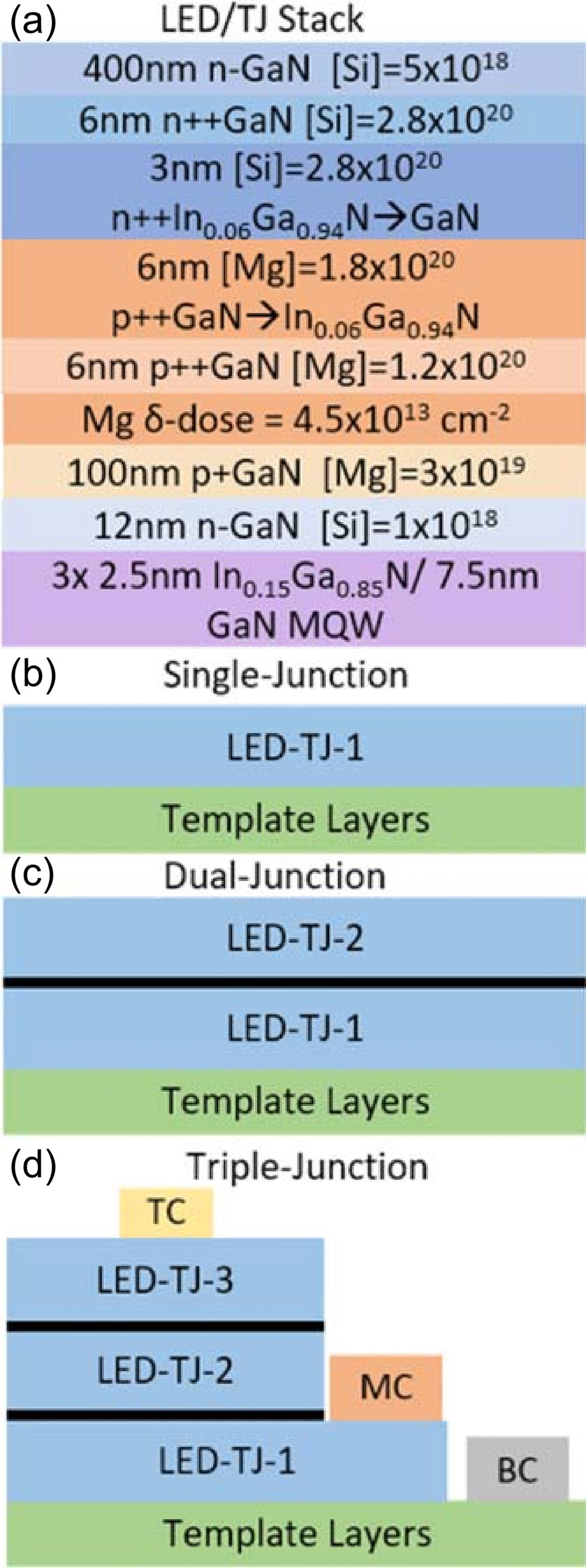
Figure 1: Epitaxial structure of (a) each LED/graded InGaN TJ period, (b) single-junction device, (c) dual-junction device, and (d) full three-junction device with top (TC), middle (MC) and bottom (BC) contacts.
The epitaxy was performed on templates consisting of sapphire substrate, 6μm n-GaN, 500nm 950°C n-GaN, and 190nm 900°C InGaN. The n-InGaN underlayer was designed to avoid V-pit defect formation.
The LEDs were fabricated with a 100μmx100μm mesa etch, p-GaN activation, and metal contact deposition. The p-GaN activation used a process developed by the team, and reported previously.
The bottom contact consisted of titanium/aluminium/nickel/gold, annealed at 850°C in nitrogen. The top ring-contact was aluminium/nickel/gold, annealed at 500°C in nitrogen. The middle contact was fabricated by etching 18μmx18μm from a corner of the device mesa and depositing aluminium/nickel/gold. This middle contact was designed to enable independent biasing of the bottom LED-TJ-1 “to probe the effects that thermal budget has on device performance”. In fact, the researchers’ measurements of forward voltage degradation suggested that dopant or indium diffusion occurred, degrading the triple-junction device’s performance.
The voltage drops for 10A/cm2 current density were 3.3V, 6.9V and 10.8V in 1-, 2- and 3-junction LEDs, respectively. The researchers point out that the increments for the TJ connections (210% for 2- and 330% for 3-junctions over 1-junction) are “significantly better than results reported earlier for MOCVD-grown cascaded LEDs for 2-junction LEDs”. The team also compares their result with a 312% increment for a 3-junction LED grown using MBE.
The Ohio/Sandia group attributes the improved junction scaling of the forward voltage to its use of a graded-composition rather than single-composition InGaN layer in the TJ structure.
On-wafer light output measurements were performed by collecting light from the sapphire side. At 50A/cm2, the peak wavlengths were 435nm, 440nm and 449nm for the single-, dual- and triple-junction wafers (Figure 2). The team suggests the differences were due to growth variations.
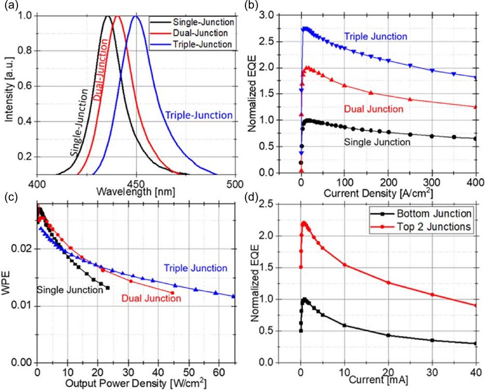
Figure 2: (a) Electroluminescence characteristics of single (black), dual (red) and triple (blue) junction devices at 50A/cm2. (b) Relative EQEs. (c) WPEs as a function of output power. (d) Relative EQEs from bottom-most junction (black), and the top 2 junctions (red) of the 3-junction LED.
The peak external quantum efficiency (EQE) of the 2-junction device was 200% that of the 1-junction’s. However, the 3-junction EQE did not scale as well, reaching a peak of only 275%. The researchers comment: “The reduction in the EQE scaling for the 3-junction device is also suspected to be a result of thermal degradation of the bottom-most LED due to the thermal budget associated with growing the 3-junction structure.”
The team broke out the EQE from the top two junctions and compared it with that from the bottom junction, using the middle contact of the 3-junction device. The top two junctions achieved an EQE more than twice that of the bottom, “suggesting a significant loss in output power for the lowest junction,” the team writes.
On the basis of a spectroscopic study showing only a slightly blue-shifted, wider peak in the bottom junction, the researchers conclude that “the thermal budget associated with the lower junction does cause a degradation in the EQE, and is an issue that could be addressed through improvements in growth techniques or active-region design.” The reduced power efficiency is attributed to an increased non-radiative recombination rate, “not captured in the electroluminescence spectra”.
Finally, the wall-plug efficiency (WPE) was estimated. The 2-junction device demonstrated superior performance over the 1-junction device above 5W/cm2 output power. The 3-junction LED had better WPE than this for output powers of 15W/cm2.
The team comments: “The improvement in WPE with increasing output power shows that multi-active-region devices can be operated at significantly higher power density while maintaining high efficiency compared with the single-junction LED.”
Triple-junction monolithic cascade structure GaN InGaN MOCVD
https://doi.org/10.35848/1882-0786/ac1981
The author Mike Cooke is a freelance technology journalist who has worked in the semiconductor and advanced technology sectors since 1997.


