


News: Optoelectronics
22 September 2021
Indium arsenide quantum dot laser for E-band dry fiber
University of Tokyo in Japan has demonstrated laser diodes emitting in the 1360-1460nm E-band range [Jinkwan Kwoen et al, Optics Express, v29, p29378, 2021]. The devices used a multi-functional metamorphic buffer (MFMB) to enable indium arsenide (InAs) quantum dot (QD) structures to operate at these wavelengths.
Until relatively recently (<20 years), the development of such devices was hindered by optical fibers for the E-band strongly attenuating transmission, due to the presence of OH groups in the glass material. Water vapor has an absorption band around 1400nm.
But now that ‘dry’ ITU-T G.652.D optical fiber resulting from new dehydration techniques has become available the search is on for efficient emitters in the E-band. Indeed, the dry fibers now give better performance than fibers designed for-O-band (1260-1360nm) transmission. The researchers also express hopes that the metamorphic technique can be applied to create optical emitters on a silicon photonics platform.
Solid-source molecular beam epitaxy (SS-MBE) on n-type (001) gallium arsenide (GaAs) substrate was used to create the InAs QD laser material. The structure included a metamorphic buffer grown on an initial 200nm GaAs buffer layer. The strained layer superlattice (SLS) consisted of three indium aluminium gallium arsenide (InAlGaAs) strained layer superlattices separated by 1.5nm AlAs to filter out threading dislocations and other defects. Each SLS consisted of 5 pairs of 10nm/10nm In0.23Al0.35Ga0.42As/In0.33Al0.35Ga0.32As sandwiched between two layers of 100nm In0.15Al0.35Ga0.50As. The AlAs interlayers were designed to avoid indium desorption during 700°C thermal annealing steps.
The laser structure was 600nm n-In0.23Al0.35Ga0.42As cladding, 50nm InAs QDs, 1500nm p-In0.23Al0.35Ga0.42As, and 400nm p- In0.23Ga0.77As contact. The QD layer consisted of 8 layers of InAs QDs in an InGaAs matrix.
Photoluminescence spectra on the structure showed a peak at 1440nm (861meV) with 44meV (74nm) full-width at half-maximum (FWHM).
Ridge lasers (Figure 1) with 6μm- and 8μm-wide mesas were fabricated (Figure 1). Sputtered silicon dioxde (SiO2) provided electrical isolation, and presumably surface passivation. The annealed electrodes consisted of gold-germanium-nickel/gold (AuGeNi/Au). The final laser bars featured 1.5mm or 2.0mm cavity length. The cleaved facets were uncoated.
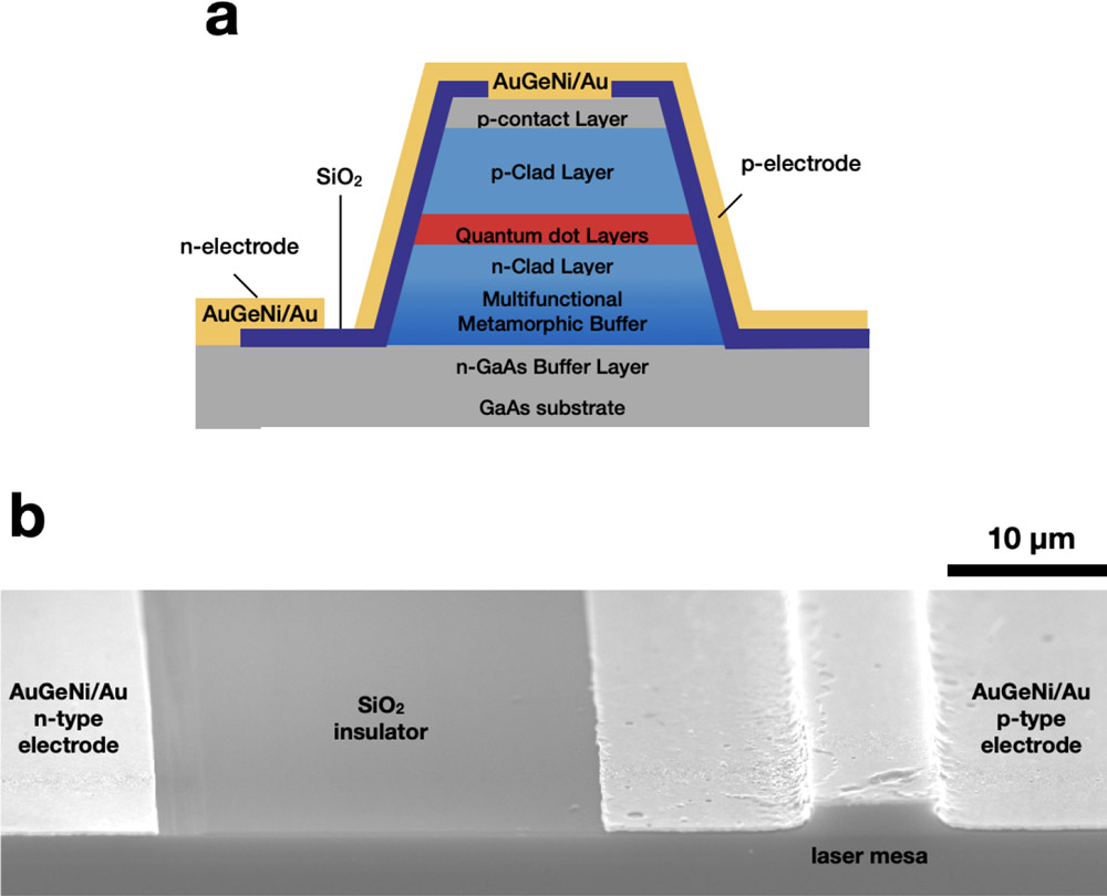
Figure 1: (a) Schematic and (b) scanning electron microscope images of InAs/InGaAs QD laser device on MFMB layer.
The metamorphic buffer allowed an increase in lattice constant from 0.56nm for GaAs to 0.575nm for In0.23Al0.35Ga0.42As. This allowed the InAs QDs to emit longer-wavelength light than usual.
The laser diodes were operated under pulsed and continuous wave (CW) modes. At 20°C, the pulse lasing threshold was 72mA, representing current density of 380A/cm2, for a 1.5mmx6μm laser diode. The threshold characteristic temperature T0 was approximately constant at 44K up to 70°C. The slope efficiency was 92.3mW/A at 20°C, 70.4mW/A at 50°C, and 23.2mW/A at 80°C.
In CW operation, the threshold was 69.2mA (360A/cm2) at 25°C on a 2mmx8μm laser diode. The researchers comment: “This is much smaller than the threshold current density of ~ 1kA/cm2 reported from InGaAsP MQW lasers and GaInNAs MQW lasers.”
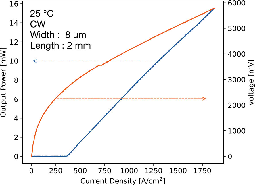
Figure 2: Output power-current-voltage (L-I-V) characteristics under CW operation at 25°C for the InAs/InGaAs QD laser on MFMB layer.
Multimode lasing was observed with a ground-state peak at 1428nm.
InAs QD laser diodes InAs GaAs substrate MBE
https://doi.org/10.1364/OE.433030
The author Mike Cooke is a freelance technology journalist who has worked in the semiconductor and advanced technology sectors since 1997.


